Search
environment

Miniaturized Laser Heterodyne Radiometer
This instrument uses a variation of laser heterodyne radiometer (LHR) to measure the concentration of trace gases in the atmosphere by measuring their absorption of sunlight in the infrared. Each absorption signal is mixed with laser light (the local oscillator) at a near-by frequency in a fast photoreceiver. The resulting beat signal is sensitive to changes in absorption, and located at an easier-to-process RF frequency. By separating the signal into a RF filter bank, trace gas concentrations can be found as a function of altitude.
sensors
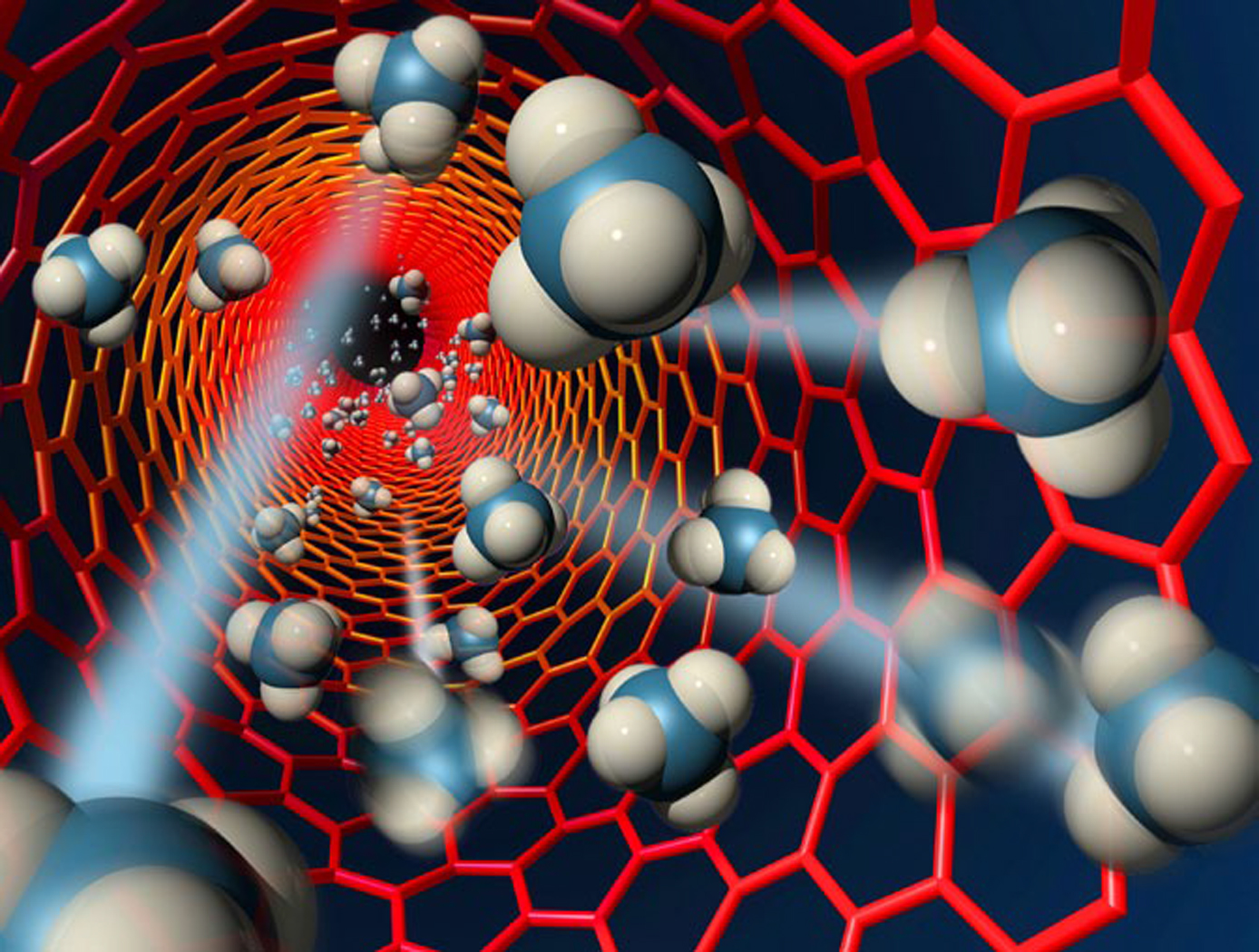
Gas Composition Sensing Using Carbon Nanotube Arrays
An array of carbon nanotubes (CNTs) in a substrate is connected to a variable-pulse voltage source. The CNT tips are spaced appropriately from the second electrode maintained at a constant voltage. A sequence of voltage pulses is applied and a pulse discharge breakdown threshold voltage is estimated for one or more gas components, from an analysis of the current-voltage characteristics. Each estimated pulse discharge breakdown threshold voltage is compared with known threshold voltages for candidate gas components to estimate whether at least one candidate gas component is present in the gas. The procedure can be repeated at higher pulse voltages to estimate a pulse discharge breakdown threshold voltage for a second component present in the gas.
The CNTs in the gas sensor have a sharp (low radius of curvature) tip; they are preferably multiwall carbon nanotubes (MWCNTs) or carbon nanofibers (CNFs), to generate high-strength electrical fields adjacent to the current collecting plate, such as a gold plated silicon wafer or a stainless steel plate for breakdown of the gas components with lower voltage application and generation of high current. The sensor system can provide a high-sensitivity, low-power-consumption tool that is very specific for identification of one or more gas components. The sensors can be multiplexed to measure current from multiple CNT arrays for simultaneous detection of several gas components.
sensors

Detection Of Presence Of Chemical Precursors
These needs are met by this invention, which provide easy stem and associated method for detecting one or more chemical precursors (components) of a multi-component explosive compound. Different carbon nanotubes (CNTs) are loaded (by doping, impregnation, coating, or other functionalization process) for detecting of different chemical substances that are the chemical precursors, respectively, if these precursors are present in a gas to which the CNTs are exposed. After exposure to the gas, a measured electrical parameter (e.g. voltage or current that correlate to impedance, conductivity, capacitance, inductance, etc.) changes with time and concentration in a predictable manner if a selected chemical precursor is present, and will approach an asymptotic value promptly after exposure to the precursor.
The measured voltage or current are compared with one or more sequence soft heir reference values for one or more known target precursor molecules, and a most probable concentration value is estimated for each one, two, or more target molecules. An error value is computed, based on differences of voltage or current for the measured and reference values, using the most probable concentration values. Where the error value is less than a threshold, the system concludes that the target molecule is likely. Presence of one, two, or more target molecules in the gas can be sensed from a single set of measurements.
sensors
Biomarker Sensor Arrays for Microfluidics Applications
This invention provides a method and system for fabricating a biomarker sensor array by dispensing one or more entities using a precisely positioned, electrically biased nanoprobe immersed in a buffered fluid over a transparent substrate. Fine patterning of the substrate can be achieved by positioning and selectively biasing the probe in a particular region, changing the pH in a sharp, localized volume of fluid less than 100 nm in diameter, resulting in a selective processing of that region. One example of the implementation of this technique is related to Dip-Pen Nanolithography (DPN), where an Atomic Force Microscope probe can be used as a pen to write protein and DNA Aptamer inks on a transparent substrate functionalized with silane-based self-assembled monolayers. But it would be recognized that the invention has a much broader range of applicability. For example, the invention can be applied to formation of patterns using biological materials, chemical materials, metals, polymers, semiconductors, small molecules, organic and inorganic thins films, or any combination of these.
sensors
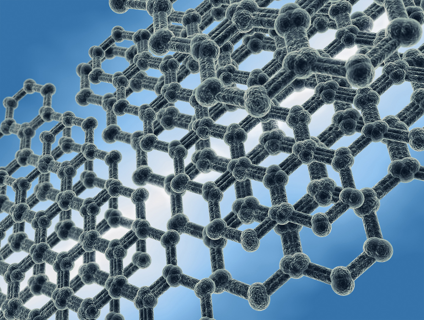
Electrical Response Using Nanotubes on a Fibrous Substrate
A resistor-type sensor was fabricated which has a network of cross-linked SWCNTs with purity over 99%. An ordinary cellulose paper used for filtration was employed as the substrate. The filter paper exhibits medium porosity with a flow rate of 60 mL/min and particle retention of 5-10m. The roughness and porosity of the papers are attractive because they increase the contact area with the ambient air and promote the adhesion to carbon nanotubes. The SWCNTs were functionalized with carboxylic acid (COOH) to render them hydrophilic, thus increasing the adhesion with the substrate. The functionalized SWCNTs were dispersed in dimethylformamide solution. The film composed of networks of cross-linked CNTs was formed using drop-cast coating followed by evaporation of the solvent. Adhesive copper foil tape was used for contact electrodes. Our sensors outperformed the oxide nanowire-based humidity sensors in terms of sensitivity and response/recovery times.
sensors
Gas Sensors Based on Coated and Doped Carbon Nanotubes
A typical sensor device includes a set of interdigitated microelectrodes fabricated by photolithography on silicon wafer or an electrically insulating substrate. In preparation for fabricating the SWCNT portion of such a sensor, a batch of treated (coated or doped) SWCNTs is dispersed in a solvent. The resulting suspension of SWCNTs is drop-deposited or injected onto the area containing the interdigitated electrodes. As the solvent evaporates, the SWCNTs form a mesh that connects the electrodes. The density of the SWCNTs in the mesh can be changed by varying the concentration of SWCNTs in the suspension and/or the amount of suspension dropped on the electrode area. To enable acquisition of measurements for comparison and to gain orthogonality in the sensor array, undoped SWCNTs can be similarly formed on another, identical set of interdigitated electrodes. Coating materials tested so far include chlorosulfonated polyethylene. Dopants that have been tested include Pd, Pt, Au, Cu and Rh nanoparticle clusters. To date, the sensor has been tested for NO2, NH3, CH4, Cl2, HCl, toluene, benzene, acetone, formaldehyde and nitrotoulene.
Sensors
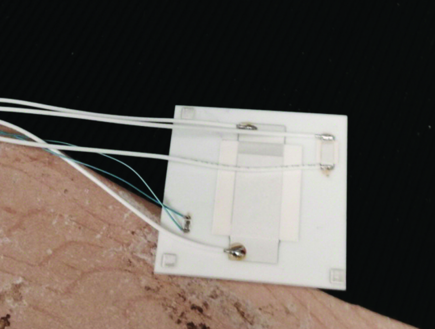
Novel Solid-State Humidity Sensor
NASAs novel ceramic dielectric material enables extremely high-sensitivity humidity sensing. The ceramic sensing element is robust, can be manufactured using printing processes, and exhibits fast response and recovery speeds with large capacitance and resistance response/change per relative humidity unit change across a wide range of humidity levels in a log-linear response. Preliminary test data conducted in a humidity test chamber show a log-linear measured response in capacitance from 5 nanofarads (at 30% relative humidity, room temperature) to 0.2 millifarads (at 90% relative humidity, room temperature).
The inventors discovered the humidity sensing element technology during their efforts to develop next-generation energy storage materials and devices for NASA. The inventors were initially puzzled by large swings in capacitance observed over the course of any given day in one particular dielectric composition, and, ultimately, they were able to trace these unexpected changes in capacitance back to corresponding changes in ambient humidity, even those occurring from breathing and exhalation.
The sensor element can be formed using a dielectric ink or paste formulation, also developed by NASA, via traditional screen printing or advanced ink jet, aerosol, or 3D printing methods. The printed sensor element can be very thin, on the order of microns in thickness, with a small footprint, one square centimeter or less.

