Search
propulsion
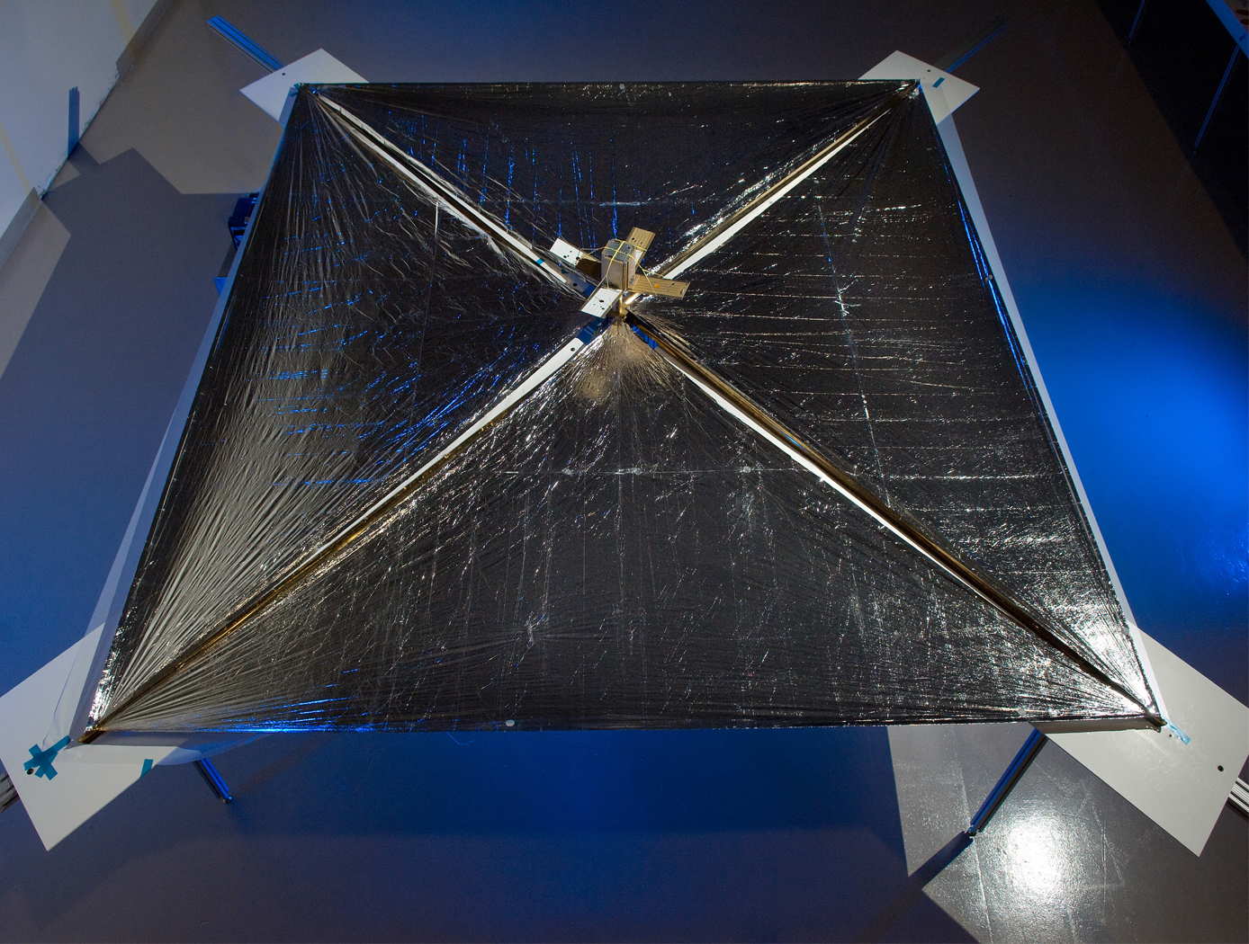
SMART Solar Sail
The SMART solar sail includes a reflective film stretched among nodes of a SMART space frame made partly of nanotubule struts. A microelectromechanical system (MEMS) at each vertex of the frame spools and unspools nanotubule struts between itself and neighboring nodes to vary the shape of the frame. The MEMSs is linked, either wirelessly or by thin wires within the struts, to an evolvable neural software system (ENSS) that controls the MEMSs to reconfigure the sail as needed. The solar sail is highly deformable from an initially highly compressed configuration, yet also capable of enabling very fine maneuvering of the spacecraft by means of small sail-surface deformations. The SMART Solar Sail is connected to the main body of the spacecraft by a SMART multi-tether structure, which includes MEMS actuators like those of the frame plus tethers in the form of longer versions of the struts in the frame.
electrical and electronics
High Mobility Transport Layer Structures for Rhombohedral Si/Ge/SiGe Devices
Performance of solar cells and other electronic devices such as transistors can be improved greatly if carrier mobility is increased. Si and Ge have Type-II bandgap alignment in cubically strained and relaxed layers. Quantum well and super lattice with Si, Ge, and SiGe have been good noble structures to build high electron mobility layer and high hole mobility layers. However, the atomic lattice constant of Ge is bigger than that of Si and direct epitaxial growth generates large density of misfit dislocations which decrease carrier mobility and shorten device life time. So it required special buffer layers such as super lattice or gradient indexed layers to grow Ge on Si wafers or Si on Ge wafers. The growth of these buffer layers takes extra effort and time such as post-annealing process to remove dislocations by dislocation gliding inside buffer layer.
This invention is a fabrication method for high mobility layer structures of rhombohedrally aligned SiGe on a trigonal substrate. The invention utilizes C-plane (0001) Sapphire which has a triangle plane, and a Si (Ge) (C) (111) crystal or an alloy of group TV semiconductor (111) crystal grown on the Sapphire.
power generation and storage

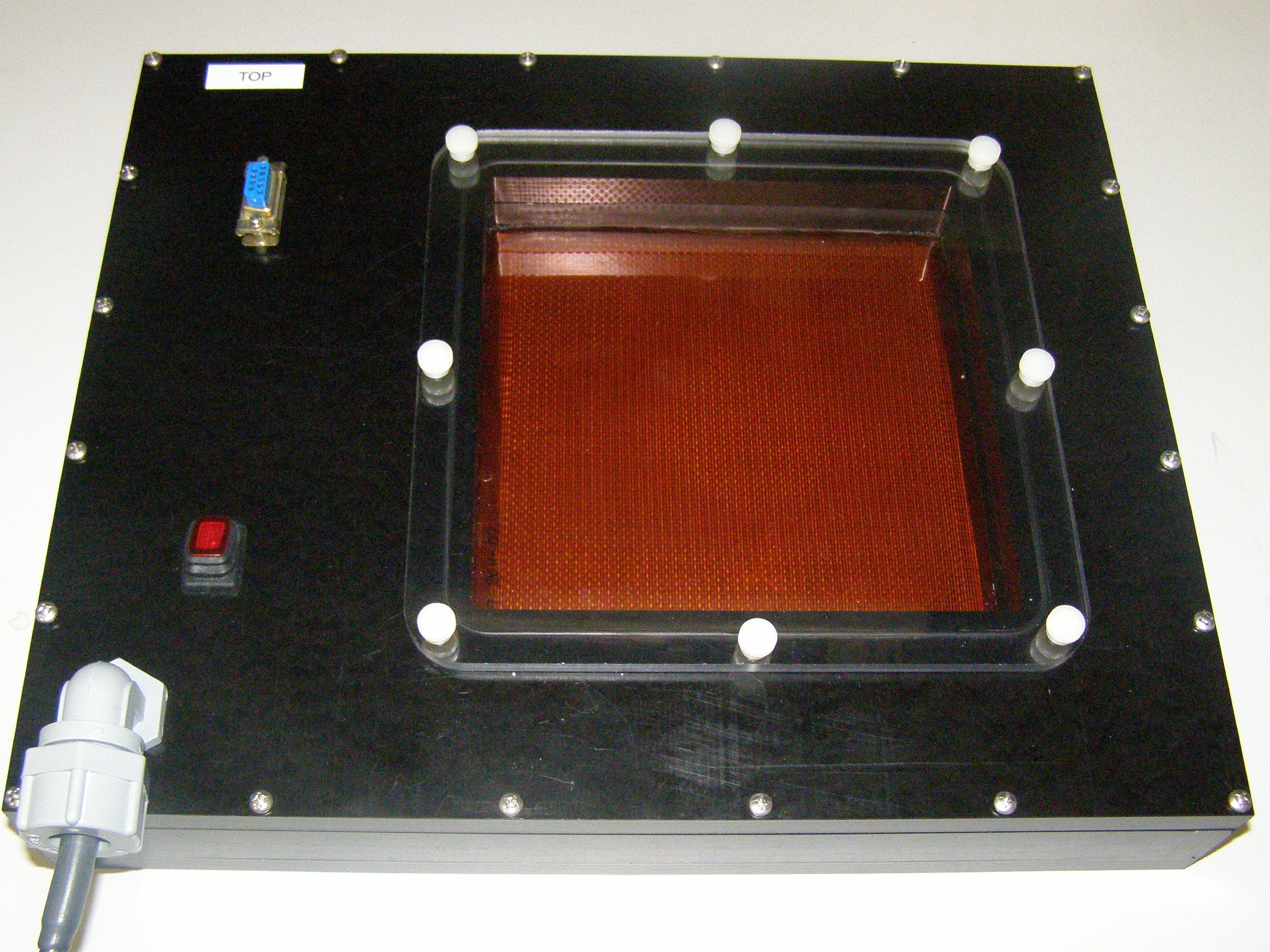
Solar Powered Carbon Dioxide (CO2) Conversion
This technology consists of a photoelectrochemical cell composed of thin metal oxide films. It uses sunlight (primarily the ultraviolet (UV), visible and Infrared (IR) portions)) and inexpensive titanium dioxide composites to perform the reaction. The device can be used to capture carbon dioxide produced in industrial processes before it is emitted to the atmosphere and convert it to a useful fuel such as methane. These devices can be deployed to the commercial market with low manufacturing and materials costs. They can be made extremely compact and efficient and used in sensor and detector applications.
sensors
Multidimensional Damage Detection System
The Damage Detection System consists of layered composite material made up of two-dimensional thin film damage detection layers separated by thicker, nondetection layers, coupled with a detection system. The damage detection layers within the composite material are thin films with a conductive grid or striped pattern. The conductive pattern can be applied on a variety of substrates using several different application methods. The number of detection layers in the composite material can be tailored depending on the level of damage detection detail needed for a particular application. When damage occurs to any detection layer, a change in the electrical properties of that layer is detected and reported. Multiple damages can be detected simultaneously, providing real-time detail on the depth and location of the damage.
The truly unique feature of the System is its flexibility. It can be designed to gather as much (or as little) information as needed for a particular application using wireless communication. Individual detection layers can be turned on or off as necessary, and algorithms can be modified to optimize performance. The damage detection system can be used to generate both diagnostic and prognostic information related to the health of layered composite structures, which will be essential if such systems are utilized to protect human life and/or critical equipment and material.
power generation and storage

Optimum Solar Conversion Cell Configurations
A solar cell manufactured from this new optical fiber has photovoltaic (PV) material integrated into the fiber to enable electricity generation from unused light, including non-visible portions of the spectrum and visible light not transmitted to a lighting application. These new solar cells are based around cylindrical optical fibers, providing two distinct advantages over the flat panels that lead to increased efficiency. The core fiber, used to transmit light, can be adjusted to increase or decrease the amount of available light that is transmitted to the lighting application at any point in real time. This invention can be applied wherever optical concentrators are used to collect and redirect incident light. Wavelengths as large as 780 nanometers (nm) can be used to drive the conversion process. This technology has very low operating costs and environmental impacts (in particular, no greenhouse gas emissions). The fiber uses low-cost polymer materials. It is lightweight and flexible, and can be manufactured using low-cost solution processing techniques. Such multifunctional materials have great potential for the future of solar and photovoltaic devices. They will enable new devices that are small and lightweight that can be used without connection to existing electrical grids.
materials and coatings

Lotus Coating
This durable, transparent, nano-textured coating can be applied via a wet chemistry process to variety of rigid and flexible surfaces by spin coating, brush application, or spray application, making it applicable for many purposes beyond space flight and aeronautical applications. The coatings unique nano-textured surface and overcoat reduces surface energy and contact surface area, giving the coating anti-contamination and self cleaning properties that minimize dust, liquid, and ice accumulation on its surface, similar to a leaf on the Lotus plant. The coating is low outgassing, stable in vacuum, and can survive harsh spaceflight environments. Depending on requirements, the Lotus Coating can be tailored to fit the specific needs of a project or customer. This customization makes the Lotus system far more adaptive, allowing for a more diverse range of applications.
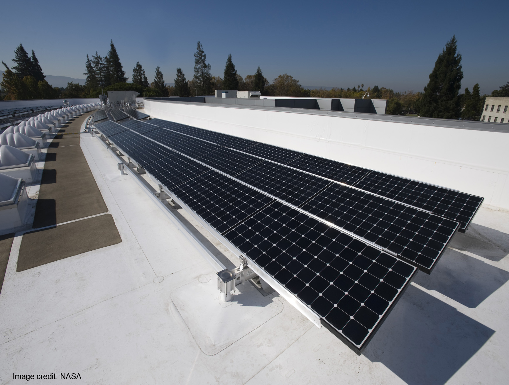
power generation and storage
High-Efficiency Solar Cell
This NASA Glenn innovation is a novel multi-junction photovoltaic cell constructed using selenium as a bonding material sandwiched between a thin film multi-junction wafer and a silicon substrate wafer, enabling higher efficiencies. A multi-junction photovoltaic cell differs from a single junction cell in that it has multiple sub-cells (p-n junctions) and can convert more of the sun's energy into electricity as the light passes through each layer. To further improve the efficiencies, this cell has three junctions, where the top wafer is made from high solar energy absorbing materials that form a two-junction cell made from the III-V semiconductor family, and the bottom substrate remains as a simple silicon wafer. The selenium interlayer is applied between the top and bottom wafers, then pressure annealed at 221°C (the melting temperature of selenium), then cooled. The selenium interlayer acts as a connective layer between the top cell that absorbs the short-wavelength light and the bottom silicon-based cell that absorbs the longer wavelengths. The three-junction solar cell manufactured using selenium as the transparent interlayer has a higher efficiency, converting more than twice the energy into electricity than traditional cells. To obtain even higher efficiencies of over 40%, both the top and bottom layers can be multi-junction solar cells with the selenium layer sandwiched in between. The resultant high performance multi-junction photovoltaic cell with the selenium interlayer provides more power per unit area while utilizing a low-cost silicon-based substrate. This unprecedented combination of increased efficiency and cost savings has considerable commercial potential.
This is an early-stage technology requiring additional development. Glenn welcomes co-development opportunities.
electrical and electronics
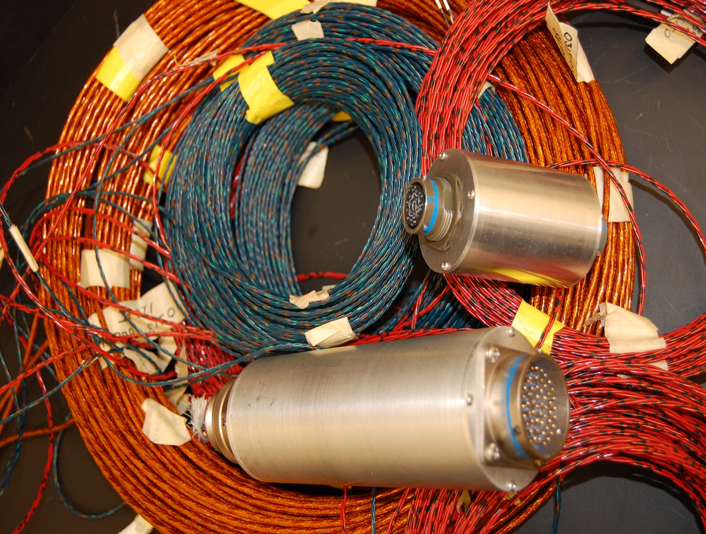
Self-Healing Wire Insulation
Insulation is necessary on electrical wires in order to protect electrical systems from shorting. In high voltage systems such shorting can lead to sparking and fires. Many lives have been lost due to electrical wire insulation failure. Many man hours are also expended in the repair and inspection of electrical wiring in order to attempt to prevent wire failure. Wire insulation with a built in "self-healing" capability would greatly improve the safety of systems containing electrical wiring. Such insulation would require far less inspection and repair time over the lifetime of the system.
Polyimides such as Kapton are an integral part of high performance electrical wire insulation. Traditional polyimides are very inert to solvents and do not melt. A new set of polyimides, developed for use as films for the manual repair of high performance electrical wire insulation, have a low melting point and can be dissolved in special solvents. These properties can be taken advantage of in self-healing polyimide films. Microcapsules containing a solvent soluble polyimide are prepared using industry standard inter-facial or in situ polymerization techniques. These capsules are then incorporated into a low melt polyimide film for use as either a primary electrical wire insulation or as one of several layers of a composite wire insulation. The low melt polyimide film substrate in which the microcapsules are incorporated has good solubility with the solvent used to dissolve the polyimide which makes up the fluid inside the microcapsule. Such a capsule filled insulation, when cut or otherwise damaged, will result in the release of the capsule contents into the cut or damage area. The solvent then dissolves a small amount of the surrounding polyimide insulation but will also begin the process of evaporation. The combination of these two processes allows for excellent intermingling of the healant and the surrounding substrate, resulting in a repair with superior bonding and physical properties.
Materials and Coatings
Self-Healing Low-Melt Polyimides
There are multiple space-related systems that can benefit from high performance, thin film, self-healing/sealing systems. Space vehicles and related ground support equipment can contain miles of wire, much of which is buried inside structures making it very difficult to access for inspection and repair. Space-based inflatable structures, solar panels, and astronauts performing extra-vehicular activities are subject to being struck by micrometeoroids and orbital debris. Self-healing or sealing layers on inflatables, solar panels and spacesuits would increase the safety and survivability of astronauts as well as the survivability and functionality of inflatables and solar panels. Self-healing insulation on wiring would greatly improve the reliability and safety of systems containing such wiring and reduce inspection and repair time over the lifetime of those systems. This technology combines the use of a self-sealing low melt, high performance polyimide film that exhibits the ability, when cut, for separated edges to slowly flow back together and seal itself, with the options of a laminate system and the inclusion of healant microcapsules that, when broken, release healant which can then additionally assist in the healing process. Combinations of the healing approaches can be enabling to the healing process proceeding at a much greater rate and dual mode healing approach can also allow for healing of a larger area.

