Search
Power Generation and Storage

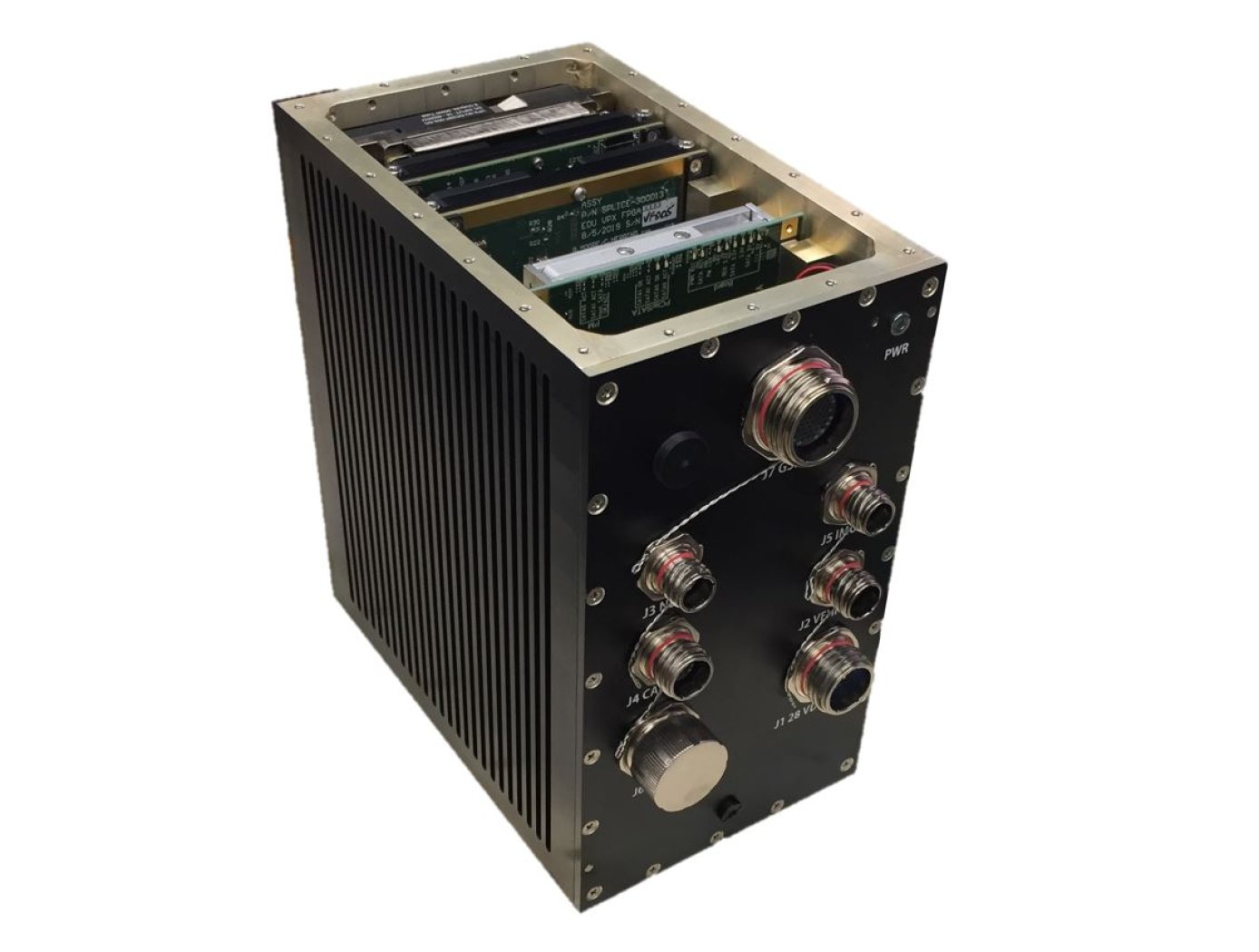
Universal Power Converter for a Lunar Power Grid
NASA’s Universal Modular Interface Converter (UMIC) is a bidirectional, modular power electronics converter that transfers power between a 120 V DC space power bus, and a medium-to-high-voltage, three-phase AC power grid. The UMIC system contains multiple parallel AC/DC UMIC modules that convert between 120 V DC and low voltage AC, as well as one or more transformers that convert power from the low voltage AC bus to the grid voltage. The UMIC module consists of multiple subsystems, including the power stage, gate driver, Field Programmable Gate Array (FPGA)-based controller, output filter, signal conditioning and sensing circuits, and thermal management subsystems. An FPGA-based controller is included within each AC/DC module and is used to regulate desired power system variables; synchronize power switching events and share load current between modules; synchronize the modules with existing service on the grid; receive commands; and share telemetry. The FPGA-based controller subsystem includes the FPGA Integrated Circuit, associated flash memory, and a controller area network (CAN) transceiver.
It is envisioned that future UMIC designs can support lunar grid expansions, a Mars surface grid, or large space stations. These applications may necessitate different grid voltages or frequencies, or different control logic and communication systems. However, the core UMIC architecture and functionality will remain the same.
The related patent is now available to license. Please note that NASA does not manufacture products itself for commercial sale.
Information Technology and Software
Unique Datapath Architecture Yields Real-Time Computing
The DLC platform is composed of three key components: a NASA-designed field programmable gate array (FPGA) board, a NASA-designed multiprocessor on-a-chip (MPSoC) board, and a proprietary datapath that links the boards to available inputs and outputs to enable high-bandwidth data collection and processing.
The inertial measurement unit (IMU), camera, Navigation Doppler Lidar (NDL), and Hazard Detection Lidar (HDL) navigation sensors (depicted in the diagram below) are connected to the DLC’s FPGA board. The datapath on this board consists of high-speed serial interfaces for each sensor, which accept the sensor data as input and converts the output to an AXI stream format. The sensor streams are multiplexed into an AXI stream which is then formatted for input to a XAUI high speed serial interface. This interface sends the data to the MPSoC Board, where it is converted back from the XAUI format to a combined AXI stream, and demultiplexed back into individual sensor AXI streams. These AXI streams are then inputted into respective DMA interfaces that provide an interface to the DDRAM on the MPSoC board. This architecture enables real-time high-bandwidth data collection and processing by preserving the MPSoC’s full ability.
This sensor datapath architecture may have other potential applications in aerospace and defense, transportation (e.g., autonomous driving), medical, research, and automation/control markets where it could serve as a key component in a high-performance computing platform and/or critical embedded system for integrating, processing, and analyzing large volumes of data in real-time.

