PCI Assembly Design
information technology and software
PCI Assembly Design (LAR-TOPS-149)
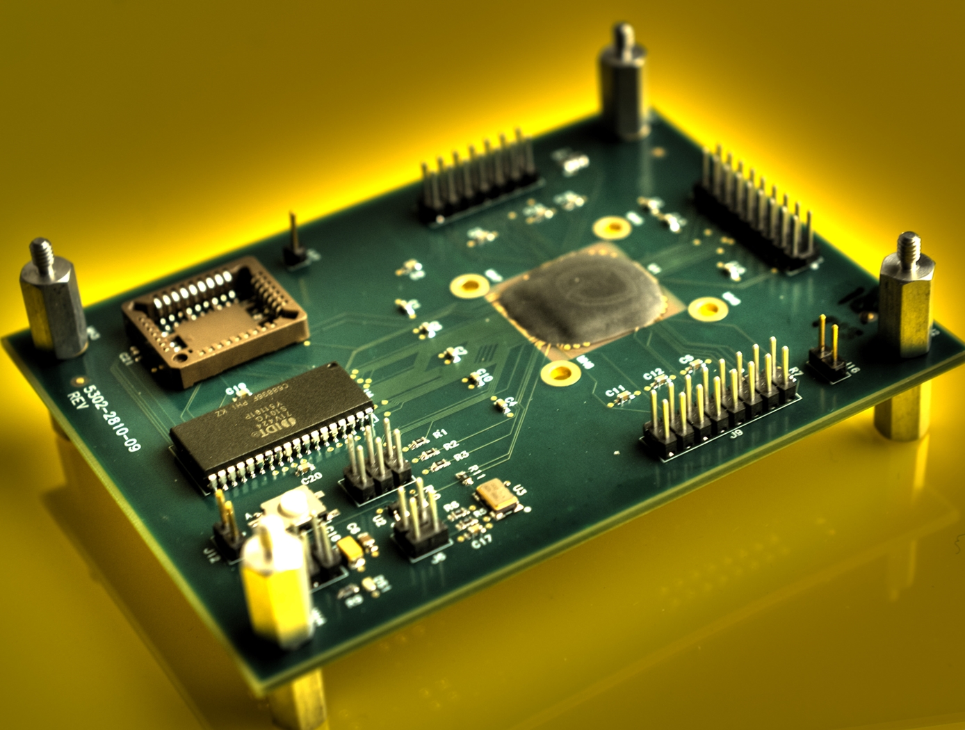
Reconfigurable peripheral component interconnect (PCI) local bus controller and target design
Overview
The invention is a design for a peripheral component interconnect (PCI) local bus controller and target in a PC/104-Plus form-factor. The design uses a flashbased field programmable gate array (FPGA) to provide immediate functionality from power-on to avoid delay after power is applied. It can be reprogrammed from connectors directly on the board, and is able to both receive and drive the clock for system and local peripherals, allowing it to function as either a PCI bus host controller or PCI target device interface. Fully compliant with the PC/104- Plus specification, the design has associated schematics and Gerber files in a vendor-ready state. The design was developed to support ongoing research in fault-tolerant computing systems.
The Technology
The PCI assembly design features flash based Field Programmable Gate Array (FPGA) technology providing in-system reprogrammable functionality from power-on. The system hosts flash-based FPGAs, SRAMs, I/O interfaces, and clocking circuitry. The circuit accommodates in-system-programming via on-board connectors, and allows functionality with separate hardware implementations with controller functionality or add-on-card functionality.


Benefits
- Simplifies design and implementation
- Reprogrammable functionality is available from the power-on state
- A single hardware assembly supports multiple functions within a computer system
Applications
- Fault-tolerant computing systems
- High-speed data acquisition
- Video acquisition
- Surveillance
- Communication gateway routers
- Embedded servers
- Intelligent transportation systems
Similar Results

Radiation Hardened 10BASE-T Ethernet Physical Interface
Currently there is no radiation hardened Ethernet interface device/circuit available commercially. In this Ethernet solution, the portion of the PHY in the FPGA is responsible for meeting the IEEE 802.3 protocol, decoding received packets and link pulses, and encoding transmitted data packets. The decoded payload data is sent to a user interface internal to the FPGA which sends data for transmission back to the FPGA PHY.
The transmit portion is composed of two AD844 op amps from Analog Devices with appropriate filtering. The receive portion is composed of a transformer, an Aeroflex Low-Voltage Differential Multi-drop device, and appropriate filtering.

SpaceCube Demonstration Platform
The HST SM4 SpaceCube flight spare was modified to create an experiment called the SpaceCube Demonstration Platform (SC DP) for use on the MISSE7 Space Station payload (in collaboration with NRL). It is designed to serve as an on-orbit platform for demonstrating advanced fault tolerance technologies.
With the use of Xilinx commercial Virtex4 FX60 FPGAs, the fault tolerant framework allows the system to recover from radiation upsets that occur in the rad-soft parts (Virtex4 FPGA logic, embedded PPCs in Virtex4 FPGAs, SDRAM and Flash), the C&DH system that runs simultaneously on both Virtex4 FPGAs that uses a robust telemetry packet structure, checksums, and the rad-hard service FPGA to validate incoming telemetry. The ability to be reconfigured from the ground while in orbit is a novel benefit, as well as is the onboard compression capabilities that allow compressed files from the ground to be uploaded to the SpaceCube.

SpaceCube
Next generation instruments are capable of producing data at rates of 108 to 1011 bits per second, and both their instrument designs and mission operations concepts are severely constrained by data rate/volume. SpaceCube is an enabling technology for these next generation missions.
SpaceCube has demonstrated enabling capabilities in Earth Science, Planetary, Satellite Servicing, Astrophysics and Heliophysics prototype applications such as on-board product generation, intelligent data volume reduction, autonomous docking/landing, direct broadcast products, and data driven processing with the ability to autonomously detect and react to events. SpaceCube systems are currently being developed and proposed for platforms from small CubeSats to larger scale experiments on the ISS and standalone free-flyer missions, and are an ideal fit for cost constrained next generation applications due to the tremendous flexibility (both functional and interface compatibility) provided by the SpaceCube system.

Game and Simulation Control
The technology is constructed to allow modulation of player inputs to a video game
or simulation from a user interface device based on the players psychophysiological
state. The invention exploits current wireless motion-sensing technologies to utilize
physiological signals for input modulation. These include, but are not limited to, heart
rate, muscle tension, and brain wave activity.
The current capability has been successfully prototyped using the Nintendo Wii
console and wireless Wii remote. The experience of electronic game play may also
be enhanced by introducing a multiplayer component in which various players
collaboratively pursue the goals of the game. The device can also enhance multiplayer
experiences such as a video game tournament, in which the skill set required in
competitive game play is increased by allowing players to interact with the game, and
compete with one another, on a psychophysiological level. This system is compatible
with the Nintendo Wii, and prototypes have been designed and are being developed
to extend this capability to the PlayStation Move, Xbox Kinect, and other
similar game platforms.

Unique Datapath Architecture Yields Real-Time Computing
The DLC platform is composed of three key components: a NASA-designed field programmable gate array (FPGA) board, a NASA-designed multiprocessor on-a-chip (MPSoC) board, and a proprietary datapath that links the boards to available inputs and outputs to enable high-bandwidth data collection and processing.
The inertial measurement unit (IMU), camera, Navigation Doppler Lidar (NDL), and Hazard Detection Lidar (HDL) navigation sensors (depicted in the diagram below) are connected to the DLC’s FPGA board. The datapath on this board consists of high-speed serial interfaces for each sensor, which accept the sensor data as input and converts the output to an AXI stream format. The sensor streams are multiplexed into an AXI stream which is then formatted for input to a XAUI high speed serial interface. This interface sends the data to the MPSoC Board, where it is converted back from the XAUI format to a combined AXI stream, and demultiplexed back into individual sensor AXI streams. These AXI streams are then inputted into respective DMA interfaces that provide an interface to the DDRAM on the MPSoC board. This architecture enables real-time high-bandwidth data collection and processing by preserving the MPSoC’s full ability.
This sensor datapath architecture may have other potential applications in aerospace and defense, transportation (e.g., autonomous driving), medical, research, and automation/control markets where it could serve as a key component in a high-performance computing platform and/or critical embedded system for integrating, processing, and analyzing large volumes of data in real-time.


