Cascaded Offset Optical Modulator
communications
Cascaded Offset Optical Modulator (LEW-TOPS-148)
For Optical Communications
Overview
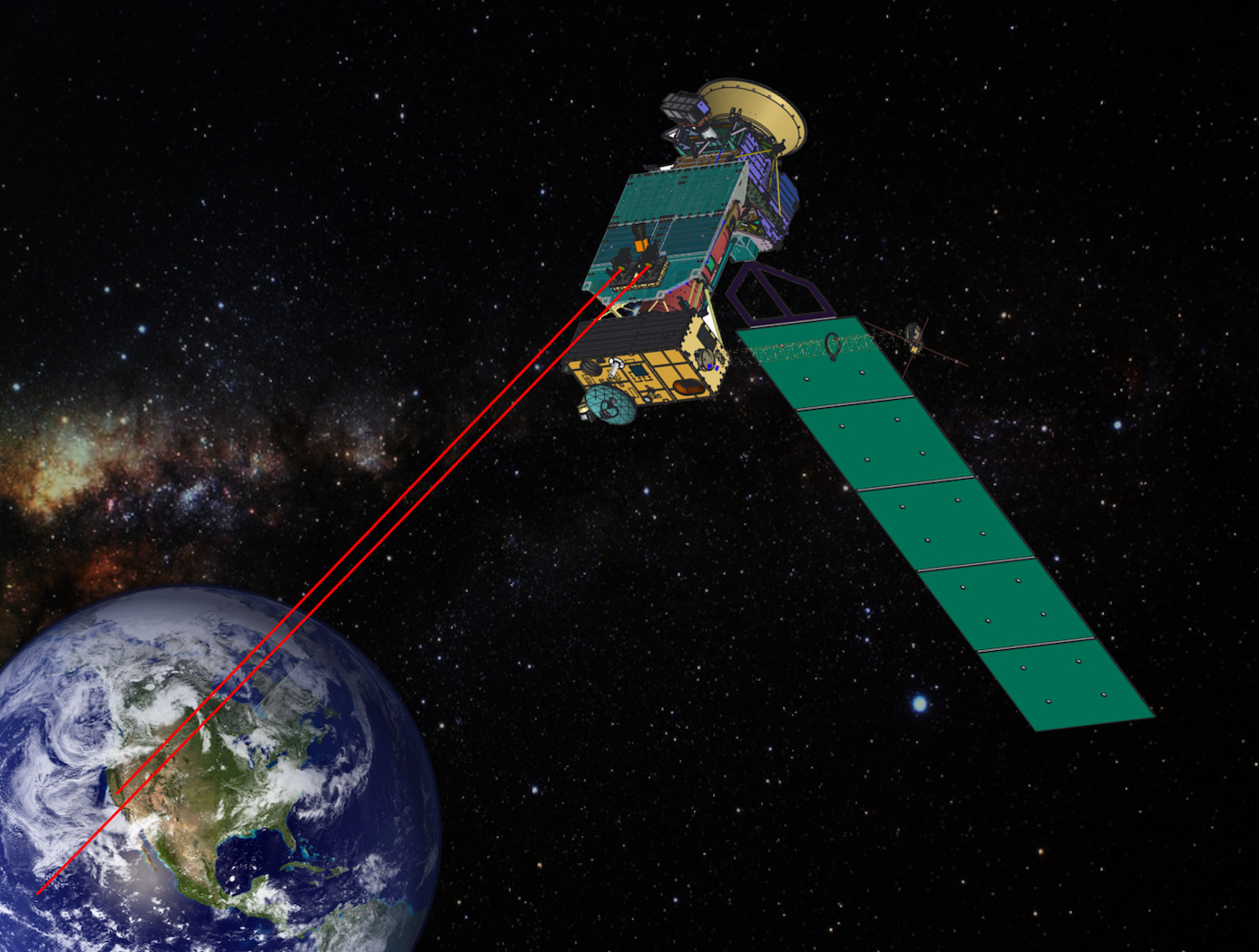
Innovators at the NASA Glenn Research Center have developed the Cascaded Offset Optical Modulator, an electro-optic subsystem used to interface a binary output Software Defined Radio (SDR) to an optical transmission system. Traditionally, this task is accomplished through the use of a Mach Zehnder Modulator (MZM), a primarily analog component. In order to generate a high-fidelity optical signal, the input electrical signal must be of equally high fidelity, which is a difficult task due to the competing requirements of the digital components and the analog modulator. The digital components required to generate the waveform contain non-idealities which degrade the extinction ratio (ER) of the optical signal. The Cascaded Offset Optical Modulator corrects these non-idealities in the electro-optic subsystem during modulation by relieving the SDR of the extreme fidelity requirements imposed by the optical modulator. This approach is valid in any optical transmission system that requires high fidelity binary pulses without a complex component.
The Technology
A unique challenge in the development of a deep space optical SDR transmitter is the optimization of the ER. For a Mars to Earth optical link, an ER of greater than 33 dB may be necessary. A high ER, however, can be difficult to achieve at the low Pulse Position Modulation (PPM) orders and narrow slot widths required for high data rates. The Cascaded Offset Optical Modulator architecture addresses this difficulty by reducing the width of the PPM pulse within the optical modulation subsystem, which relieves the SDR of the high signal quality requirements imposed by the use of an MZM. With the addition of a second MZM and a variable time delay, all of the non-idealities in the electrical signal can be compensated by slightly offsetting the modulation of the laser. The pulse output is only at maximum intensity during the overlap of the two MZMs. The width of the output pulse is effectively reduced by the offset between MZMs. Measurement and analysis of the system displayed, for a 1 nanosecond pulse width, extinction ratios of of 32.5 dB, 39.1 dB, 41.6 dB, 43.3 dB, 45.8 dB, and 48.2 dB for PPM orders of 4, 16, 32, 64, 128, and 256, respectively. This approach is not limited to deep space optical communications, but can be applied to any optical transmission system that requires high fidelity binary pulses without a complex component. The system could be used as a drop-in upgrade to many existing optical transmitters, not only in free space, but also in fiber. The system could also be implemented in different ways. With an increase in ER, the engineer has the choice of using the excess ER for channel capacity, or simplifying other parts of the system. The extra ER could be traded for reduced laser power, elimination of optical amplifiers, or decreased system complexity and efficiency.

Benefits
- Reduced complexity for optical modulators in Pulse Position Modulation (PPM) systems: The Cascaded Offset Optical Modulator reduces the signal quality requirement for the SDR, resulting in a less complex and more cost effective implementation
- Increased channel capacity and reduced SWaP: This innovation simplifies the electrical portion of an electro-optic system, which can significantly increase channel capacity and reduce size, weight, and power (SWaP)
- High-quality PPM signal: The Cascaded Offset Optical Modulator has achieved a signal with a 40 dB extinction ratio for PPM32 and a 48 db extinction ration for PPM256
- Compatible with current communications infrastructure: Drop-in upgrade to many existing optical transmitters in free space and fiber
Applications
- Free-space optical communications
- Fiber-optic communications
Technology Details
communications
LEW-TOPS-148
LEW-19698-1
Patent Pending
"Optical Software Defined Radio Transmitter Extinction Ratio Enhancement with Differential Pulse Carving," Lantz, Nicholas C., et al., February 2, 2019,
https://ntrs.nasa.gov/search.jsp?R=20190025712
https://ntrs.nasa.gov/search.jsp?R=20190025712
|
Tags:
|
Similar Results

Dynamic Range Enhancement of High-Speed Data Acquisition Systems
Electronic waveforms exist that exceed the capabilities of state-of-the-art data acquisition hardware that is commonly available. The electronic waveforms that need to be measured simultaneously contain wide bandwidth, high frequency content, a DC reference, high dynamic range, and a high crest factor. The NASA Glenn high-speed data acquisition system creates a voltage compression effect with a custom transfer function that is adapted to the voltage range, frequency bandwidth, and electrical impedance of both the test article and data acquisition device. The compression transfer function is later reversed (or decompressed) with a software algorithm to restore the original signal's voltage from the acquired data. The data is thus improved via better signal-to-noise ratio, better low-amplitude accuracy, better resolution, and preservation of high-frequency spectral content. The circuit can be realized with either passive components or both active and passive components. Either realization is specialized for the test article and data acquisition hardware.
This is an early-stage technology requiring additional development. Glenn welcomes co-development opportunities.

Multimode Directional Coupler
Glenn's researchers originally created the MDC to improve the beacon sources for atmospheric propagation studies. These studies are typically conducted to test atmospheric conditions to determine the signal strength needed for satellite communications. A low-power transmitter (e.g., a beacon source) is attached to the satellite, and transmits a continuous waveform (CW) signal to a receiving station on Earth. However, when a separate frequency is desired, building a new beacon source for the transmitter on the satellite - especially one that will operate at higher frequencies - presents numerous challenges. For one, a single-frequency beacon source requires a temperature-stabilized oscillator for frequency generation separate from that provided by the spacecraft receiver.
To solve such problems, Glenn's innovators fabricated the MDC from two sections of waveguide: a primary waveguide for the fundamental frequency (Ku-band), and a secondary waveguide for the harmonics (Ka-band). These sections are joined together so that precision-machined slots in the second waveguide selectively couple the harmonics, for amplification and transmission. The harmonics can then be used as an additional beacon source with very small power losses to the fundamental signal. Once the separation takes place, the second or higher harmonic can be amplified and transmitted to a station on Earth. The efficiency and performance of the MDC can be optimized through appropriate computer modeling software and currently available high-precision fabrication techniques. Without the complexity and expense involved in building separate traveling wave tube amplifiers to generate additional frequencies, Glenn's MDC enables satellites to produce multiple signals that can be received by multiple stations - a significant leap forward in satellite productivity.

Serial Arrayed Waveguide Grating
Serial Arrayed Waveguide Grating enables higher resolution wavelength separation. Traditional AWGs split the optical signal into multiple parallel paths each with a different path length. This new approach creates the different path lengths by splitting the signal into essentially one long path in which the different channels are periodically split off the main path in the desired fraction. This has the net result of requiring much less space on-chip for comparable optical path differences.
In traditional AWG, there are multiple parallel optical paths, each with a different engineered path-length. For high resolution, you want many different parallel paths and large differences in path length between the paths. To design this on a photonics chip requires significant area. The serial AWG creates a single path, equivalent to the longest path in the parallel AWG and split off fractions of the optical signal at various points along the way to create the equivalent path lengths. Serial Arrayed Waveguide Grating re-uses the same path instead of needing independent parallel paths.

Tunable Multi-Tone, Multi-Band, High-Frequency Synthesizer
Glenn's revolutionary new multi-tone, high-frequency synthesizer can enable a major upgrade in the design of high data rate, wide-band satellite communications links, in addition to the study of atmospheric effects. Conventional single-frequency beacon transmitters have a major limitation: they must assume that atmospheric attenuation and group delay effects are constant at all frequencies across the band of interest. Glenn's synthesizer overcomes this limitation by enabling measurements to be made at multiple frequencies across the entire multi-GHz wide frequency, providing much more accurate and actionable readings.
This novel synthesizer consists of a solid-state frequency comb or harmonic generator that uses step-recovery semiconductor diodes to generate a broad range of evenly spaced harmonic frequencies, which are coherent and tunable over a wide frequency range. These harmonics are then filtered by a tunable bandpass filter and amplified to the necessary power level by a tunable millimeter-wave power amplifier. Next, the amplified signals are transmitted as beacon signals from a satellite to a ground receiving station. By measuring the relative signal strength and phase at ground sites the atmospheric induced effects can be determined, enabling scientists to gather essential climate data on hurricanes and climate change. In addition, the synthesizer can serve as a wideband source in place of a satellite transponder, making it easier to downlink high volumes of collected data to the scientific community. Glenn's synthesizer enables a beacon transmitter that, from the economical CubeSat platform, offers simultaneous, fast, and more accurate wideband transmission from space through the Earth's atmosphere than has ever been possible before.

Compact, Temperature-Tuned OFDR Laser
Because OFDR-based fiber interrogation systems rely upon interferometry between sensors with respect to a unique reference length, the excitation source (laser) must lase at a single longitudinal mode (SLM). If the excitation source contains multiple modes, the resulting beat frequency becomes a super-position of the multiple frequencies caused by the modes; as a result, the sensor cannot be accurately defined in the Fourier domain. For OFDR systems with high sensing ranges, a continuous wavelength tunable laser must be used to accommodate the resonant wavelength shift of the fiber sensors due to environmental changes. External cavity lasers (ECLs) have been used due to their narrow linewidth and ability to lase at a SLM with no mode-hopping between steps. However, the mechanical complexity associated with tuning, susceptibility to vibration and shock, and high price point leave much to be desired.
To overcome the limitations of OFDR-based FOSS systems resulting from non-ideal excitation sources, NASA has developed a narrow linewidth solid-state laser based on the Distributed Feedback (DFB) laser. NASAs laser is continuously tuned by manipulating the laser cavitys temperature via a thermal-electric cooler feedback system. This continuous wavelength tuning generates a clean clock signal within an auxiliary interferometer, while the laser simultaneously interrogates multiple FBGs to produce a clean sensing interferometer. A Fourier domain spectrograph is used to show the unique frequency (i.e., location) of each FBG.
While NASAs excitation source provides several performance advantages over conventional lasers used in OFDR, it is also highly compact and one eighth the cost of the ECLs traditionally used as excitation sources in OFDR-based systems. The laser has no moving parts, which also substantially improves system reliability.
Originally developed to demonstrate a low-cost interrogator for liquid level sensing in oil tanks, NASAs compact, temperature-tuned OFDR laser can be applied wherever OFDR-based fiber optic sensing is desirable. Additional applications may include temperature distribution sensing, strain sensing, pressure sensing, and more.
NASA AFRC has strong subject matter expertise in fiber optic sensing systems, and has developed several patented technologies that are available for commercial licensing. For more information about the full portfolio of FOSS technologies, visit:
https://technology-afrc.ndc.nasa.gov/featurestory/fiber-optic-sensing

