Highly secure all-printed Physically Unclonable Function (PUF) electronic device based on a nanomaterial network
Electrical and Electronics
Highly secure all-printed Physically Unclonable Function (PUF) electronic device based on a nanomaterial network (TOP2-317)
Leveraging inherent variability in nanomaterial networks to create a simple, low-cost, durable, and easy to manufacture PUF for secure authentication
Overview
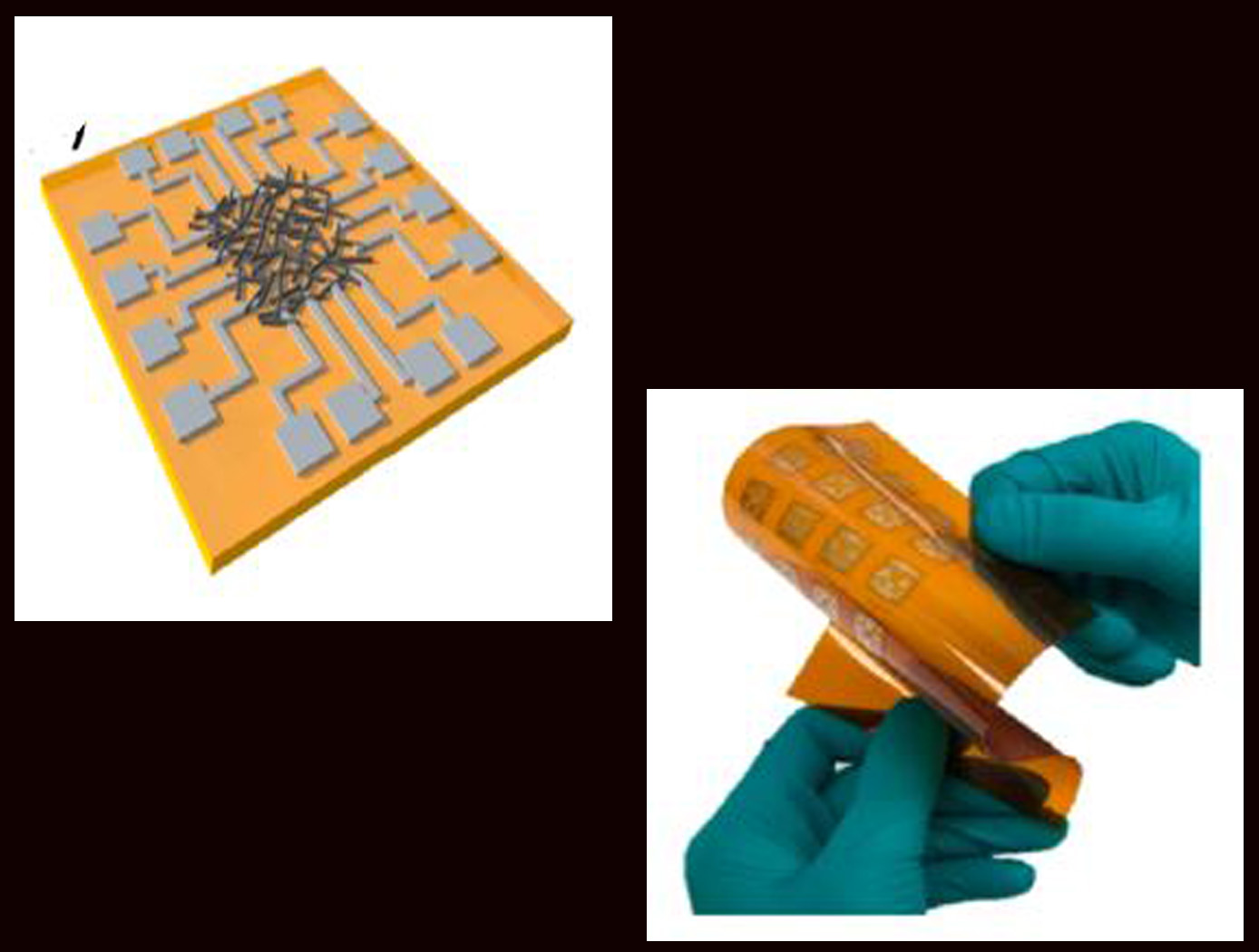
Assets are traditionally secured so important information can only be accessed when a key is placed in a lock (physical or electronic). Given the tremendous increase in the number of devices in the era of Internet of Things (IoT), direct access between things without human intervention is ideal. IoT related devices require unique identification codes that can be safely stored for security and that are resistant to physical attacks and exposure to harsh environments. As a solution, NASA Ames has developed a Physically Unclonable Function (PUF) electronic device using an all-printed nanomaterial network , such as a Carbon Nanotube (CNT) network. The invention leverages the intrinsic, random, and unique features of CNTs in a network for authentication, which can be used as a secret, stable, and robust key for high-level hardware security.
The Technology
The technology is an all-printed Physically Unclonable Function (PUF) electronic device based on a nanomaterial (such as single-walled carbon nanotube) network. The network may be a mixture of semiconducting and metallic nanotubes randomly tangled with each other through the printing process. The all-printed PUF electronic device comprises a nanomaterial ink that is inkjet deposited, dried, and randomly tangled on a substrate, creating a network. A plurality of electrode pairs is attached to the substrate around the substrate perimeter. Each nanotube in the network can be a conduction path between electrode pairs, with the resistance values varying among individual pairs and between networks due to inherent inter-device and intra-device variability. The unique resistance distribution pattern for each network may be visualized using a contour map based on the electrode information, providing a PUF key that is a 2D pattern of analog values. The PUF security keys remain stable and maintain robustness against security attacks. Although local resistance change may occur inside the network (e.g., due to environmental impact), such change has little effect on the overall pattern. In addition, when a network-wide resistance change occurs, all resistances are affected together, so that the unique pattern is maintained.
 Conventional lumped electrode configuration. (b) Distributed electrode configuration. (c) Box plot with whiskers from minimum to maximum. The middle line of the box plot represents the median of the CNT resistances.")
Benefits
- Low-cost fabrication
- Durable
- Easy to manufacture
- Stable, resistant to environmental impacts and tampering
- Includes a method of reading multiple resistances by placing multiple electrodes around a single CNT network
- Inter-device and intra-device (device-to-device) variability is harnessed here for the PUF application
- Flexible and printable electronics for portable or wearable devices will be networked to meet the IoT era demands
- Security key cannot be duplicated or identified without access to the secure device
Applications
- Thin film transistors
- Energy storage devices
- Displays and sensors
- Portable or wearable devices
- Internet of Things (IoTs)
Technology Details
Electrical and Electronics
TOP2-317
ARC-18241-1
ARC-18241-2
https://www.researchgate.net/publication/333758580_Physically_Unclonable_Function_by_an_All-Printed_Carbon_Nanotube_Network
“Patent only, NO software available.”
|
Tags:
|
|
|
Related Links:
|
Similar Results

Gas Sensors Based on Coated and Doped Carbon Nanotubes
A typical sensor device includes a set of interdigitated microelectrodes fabricated by photolithography on silicon wafer or an electrically insulating substrate. In preparation for fabricating the SWCNT portion of such a sensor, a batch of treated (coated or doped) SWCNTs is dispersed in a solvent. The resulting suspension of SWCNTs is drop-deposited or injected onto the area containing the interdigitated electrodes. As the solvent evaporates, the SWCNTs form a mesh that connects the electrodes. The density of the SWCNTs in the mesh can be changed by varying the concentration of SWCNTs in the suspension and/or the amount of suspension dropped on the electrode area. To enable acquisition of measurements for comparison and to gain orthogonality in the sensor array, undoped SWCNTs can be similarly formed on another, identical set of interdigitated electrodes. Coating materials tested so far include chlorosulfonated polyethylene. Dopants that have been tested include Pd, Pt, Au, Cu and Rh nanoparticle clusters. To date, the sensor has been tested for NO2, NH3, CH4, Cl2, HCl, toluene, benzene, acetone, formaldehyde and nitrotoulene.

Holey Carbon Allotropes
This invention is for scalable methods that allows preparation of bulk quantities of holey nanocarbons with holes ranging from a few to over 100 nm in diameter. The first method uses metal particles as a catalyst (silver, copper, e.g.) and offers a wider range of hole diameter. The second method is free of catalysts altogether and offers more rapid processing in a single step with minimal product work-up requirements and does not require solvents, catalysts, flammable gases, additional chemical agents, or electrolysis. The process requires only commercially available materials and standard laboratory equipment; and, it is scalable. Properties that can be controlled include: surface area, pore volume, mechanical properties, electrical conductivity, and thermal conductivity.

Conductive Polymer/Carbon Nanotube Structural Materials and Methods for Making Same
Carbon nanotubes (CNTs) show promise for multifunctional materials for a range of applications due to their outstanding combination of mechanical, electrical and thermal properties. However, these promising mechanical properties have not translated well to CNT nanocomposites fabricated by conventional methods due to the weak load transfer between tubes or tube bundles.
In this invention, the carbon nanotube forms such as sheets and yarns were modified by in-situ polymerization with polyaniline, a -conjugated conductive polymer. The resulting CNT nanocomposites were subsequently post-processed to improve mechanical properties by hot pressing and carbonization. A significant improvement of mechanical properties of the polyaniline/carbon nanotube nanocomposites was achieved through a combination of stretching, polymerization, hot pressing, and carbonization.

Inexpensive Microsensor Fabrication Process
Because chemical sensors are used in many aspects of space missions, NASA researchers are continually developing ever smaller and more robust sensors that can be manufactured inexpensively and in high quantities; e.g., in batches. Glenn has developed a way to inexpensively fabricate microsensors using a sacrificial template approach. A nanostructure, such as a carbon nanotube, serves as a template, which can then be coated with a high-temperature oxide material. The carbon nanotube can be burned off, or sacrificed, leaving only the metal oxide. The resulting structure provides the unique morphology and properties of the carbon nanotube, which are advantageous for sensing, along with the material durability and high-temperature sensing capabilities of the metal oxide. This technique increases the surface area available for sensing because both the interior and exterior of the resulting microsensor can be used for gas detection, significantly increasing performance.
The fabrication of these microsensors includes three major steps: (1) synthesis of the porous metal or metal oxide nanostructures using a sacrificial template, (2) deposition of the electrodes onto alumina substrates, and (3) alignment of the nanostructures between the electrodes. The invention has been demonstrated for methane detection at room temperature (using tin oxide, with carbon nanotubes as the sacrificial template). The microsensor offers low power consumption (no heating required), compact size, extremely low cost, and simple batch-fabrication.

Filtering Molecules with Nanotube Technology
This water filtration innovation is an acoustically driven molecular sieve embedded with small-diameter carbon nanotubes. First, water enters the device and contacts the filter matrix, which can be made of polymer, ceramic, or metallic compounds. Carbon nanotubes within the matrix allow only water molecules to pass through, leaving behind any larger molecules and contaminants. The unique aspect of the technology is its use of acoustics to help drive water through the filter.
An oscillator circuit attached to the filter matrix propagates acoustic vibration, further causing water molecules to de-bond and move through the filter. This use of acoustics also eliminates dependence on gravity (and thus filter orientation) to move water through the device. When water exiting the system diminishes to a pre-determined set point, a cleaning cycle is triggered to clear the sediment from the inlet of the filter, reestablishing the standard system flow rate. Unlike other filtration systems, flushing of the filter system is not required. The combination of acoustics and small-diameter carbon nanotubes in this innovation make it an effective and efficient means of producing contaminant-free, clean water.

