Search
Materials and Coatings

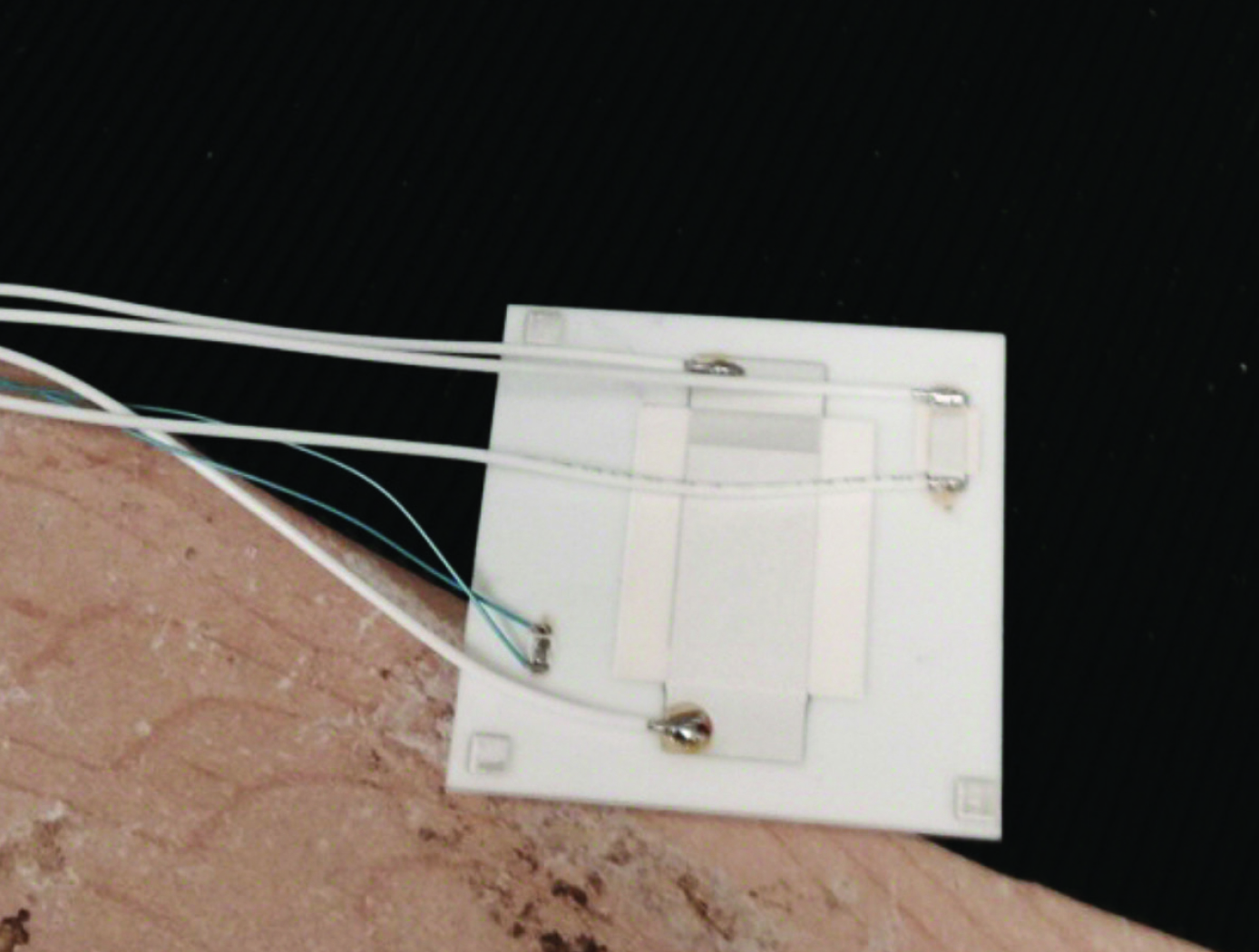
Self-Cleaning Coatings for Space or Earth
The new transparent EDS technology is lighter, easier to manufacture, and operates at a lower voltage than current transparent EDS technologies. The coating combines an optimized electrode pattern with a vapor deposited protective coating of SiO2 on top of the electrodes, which replaces either polymer layers or manually adhered cover glass (see figure on the right). The new technology has been shown to achieve similar performances (i.e., over 90% dust clearing efficiency) to previous technologies while being operated at half the voltage.
The key improvement of the new EDS coating comes from an innovative method to successfully deposit a protective layer of SiO2 that is much thinner than typical cover glass. Using vapor deposition enables the new EDS to scale more successfully than other technologies that may require more manual manufacturing methods. The EDS here has been proven to reduce dust buildup well under vacuum and may be adapted for terrestrial uses where cleaning is done manually. The coatings could provide a significant improvement for dust removal of solar cells in regions (e.g., deserts) where dust buildup is inevitable, but water access is limited. The EDS may also be applicable for any transparent surface that must remain transparent in a harsh or dirty environment.
The related patent is now available to license. Please note that NASA does not manufacturer products itself for commercial sale.
Materials and Coatings

Non-Magnetic Absorptive Material for Microwave to Far-Infrared Applications
The electromagnetic properties of the material are engineered by optimizing its complex dielectric function through the volume filling fraction of its components. A low-index polymeric binder, such as thermal polymers and epoxies, serves as the host medium to minimize reflectance in the conductively loaded dielectric media. To ensure thermal compatibility with metal substrates in cryogenic environments, dielectric powders are incorporated to match thermal expansion. Additionally, alumina frit compensates for thermal contraction at cryogenic temperatures, while non-magnetic conductive particles such as bronze, carbon allotropes, and degenerately doped silicon help tailor the material’s dielectric response.
To enhance performance, small-particle scatterers reduce heat capacity and limit resonant dispersion, while dirty alloys stabilize resistance under conductive loading. The formulation incorporates reststrahlen materials and supports applications across the microwave to terahertz range, making it suitable for baffles, Lyot stops, and optical terminations, or as a primer for enhancing near-infrared and visible black paints.
This high-emissivity, non-magnetic coating is designed for microwave to far-infrared instrumentation in space and cryogenic systems. It also benefits industries producing absorptive epoxies, EMI/EMC shielding, and quantum sensing components. It has reached Technology Readiness Level (TRL) 5 (component validation in relevant environment) and is now available for patent licensing.
Sensors
Novel Solid-State Humidity Sensor
NASAs novel ceramic dielectric material enables extremely high-sensitivity humidity sensing. The ceramic sensing element is robust, can be manufactured using printing processes, and exhibits fast response and recovery speeds with large capacitance and resistance response/change per relative humidity unit change across a wide range of humidity levels in a log-linear response. Preliminary test data conducted in a humidity test chamber show a log-linear measured response in capacitance from 5 nanofarads (at 30% relative humidity, room temperature) to 0.2 millifarads (at 90% relative humidity, room temperature).
The inventors discovered the humidity sensing element technology during their efforts to develop next-generation energy storage materials and devices for NASA. The inventors were initially puzzled by large swings in capacitance observed over the course of any given day in one particular dielectric composition, and, ultimately, they were able to trace these unexpected changes in capacitance back to corresponding changes in ambient humidity, even those occurring from breathing and exhalation.
The sensor element can be formed using a dielectric ink or paste formulation, also developed by NASA, via traditional screen printing or advanced ink jet, aerosol, or 3D printing methods. The printed sensor element can be very thin, on the order of microns in thickness, with a small footprint, one square centimeter or less.
Materials and Coatings

Waveguide-based Dielectric and Magnetic Property Measurement
This NASA invention utilizes a simple waveguide-based measurement system to determine the complex dielectric permittivity and magnetic permeability of arbitrary-shaped planetary rock samples. The system operates at L-band frequencies (~1 GHz) and can be extended to P- and S-bands for broader applications. The approach involves placing an arbitrarily-shaped sample inside an open-ended waveguide excited by a coaxial probe, measuring the scattering parameters, and extracting dielectric and magnetic properties through computational modeling and optimization techniques.
A key aspect of this system is its ability to handle non-uniform and irregularly shaped rock samples, enabling the measurement of real-world planetary materials without requiring extensive sample preparation. The methodology includes calibration in an anechoic chamber, computational modeling, and iterative refinement of measured vs. simulated scattering parameters to extract the material properties.
Future advancements will involve expanding measurements to different frequency bands, refining computational models using artificial intelligence, and automatically rotating samples within the waveguide to obtain multiple directional measurements (enhancing precision while reducing test time).
This NASA innovation has been successfully applied to two Martian meteorite samples, yielding values of dielectric permittivity and permeability relevant for Mars radar applications. The system will further be leveraged to build an expansive database of the dielectric properties of planetary soils and rocks to improve radar-based mapping (e.g., subsurface mapping) missions. The invention could also be applied for the non-destructive screening of a variety of samples using radio waves, including biological samples for medical purposes, additive manufacturing feedstock or finished parts, and mining-related rock samples to test for impurities or resources of interest. This NASA invention is at technology readiness level (TRL) 5 (component and/or breadboard validation in relevant environment) and is available for patent licensing.

