Search
Manufacturing

Fabrication of Binary Phase Photon Sieves
This NASA invention is an innovative process for fabricating high-area binary phase photon sieves with improved optical efficiency for EUV imaging applications. Binary phase photon sieves have been demonstrated for a variety of optical and x-ray applications. Photon sieves must be wide, super-thin, and etched with precise holes to refract light. Each step in NASA's photon sieve fabrication process includes considerations to protect the resulting sieves, such as leaving a honeycomb of thicker material to support the membrane and prevent tearing. The process starts by using a silicon-on-insulator wafer, includes pattern and etch-sieve pattern, and ends with a released photon sieve. The inventors have produced an 8 cm-diameter silicon sieve that is 100 nm thick including hole sizes of 2 µm in diameter with 2 µm spacing. Additionally, a similar structure has been demonstrated in niobium, with 8 cm in diameter with the same silicon hexagonal support frame.
This novel process enables the fabrication of photon sieves for EUV imaging applications. While the process was initially developed to fabricate photon sieves for solar science and astronomy, it could also be used to generate metamaterial/frequency selective surface structures from the UV to THz frequency ranges. This NASA invention is a Technology Readiness Level (TRL) 4 (prototype validation in a laboratory environment) technology and is available for patent licensing.
Manufacturing

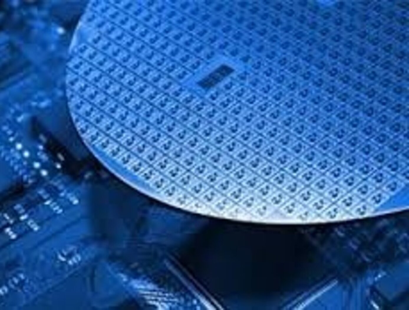
Ultra-low Reflectivity Black Silicon Pupil Masks
Fabrication of NASA's pupil mask begins with the preparation of a silicon wafer, which serves as the foundation for the black silicon structure. The wafer undergoes ion beam figuring (IBF), a non-contact technique that precisely removes surface irregularities at the nanometer scale. This process ensures that the silicon surface is diffraction-limited, eliminating errors that could degrade optical performance. Once the wafer is polished to the required precision, it is then processed lithographically to define the mask pattern, creating reflective and absorptive regions essential for controlling light propagation.
To achieve the desired high absorption characteristics, the lithographically patterned wafer undergoes cryogenic etching, a sophisticated process that transforms the silicon surface into a highly textured, black silicon structure. This method utilizes a controlled plasma environment with sulfur hexafluoride (SF6) and oxygen to etch the surface at cryogenic temperatures. The process is carefully optimized by adjusting parameters such as gas flow rates, chamber pressure, ion density, and etch duration, leading to the formation of high-aspect-ratio nanostructures on the silicon substrate. These structures, resembling a dense “forest” of silicon nanospikes, trap and diffuse incoming light, drastically reducing specular reflection. The resulting surface exhibits an ultra-low reflectivity that is orders of magnitude lower than conventional polished silicon.
By leveraging NASA’s cutting-edge fabrication technique, the newly developed black silicon pupil mask offers a powerful solution for high-contrast astronomical imaging. Its ability to minimize scattered light and enhance optical contrast makes it an ideal component for space telescopes tasked with directly imaging exoplanets as well as other applications requiring ultra low reflectivity systems.
Materials and Coatings
Epitaxy of SiGe and Other Compound Semiconductors
Several of the patented methods included in this suite of technologies enable super-hetero-epitaxy of rhombohedral/cubic compound semiconductors on specially oriented trigonal (e.g. sapphire) or hexagonal (e.g. quartz) crystal wafer substrates. This includes alignment of the growth crystal lattice with the underlying substrate lattice to minimize misfit strain-induced dislocation defects in the growing crystal. Thus thicker, defect-free crystal layers can be made. Rhombohedral/Cubic crystal twin defects which is 60 degree rotated on [111] orientation in a rhombohedral/cubic SiGe layer structure can be reduced to well less than 1% by volume, essentially providing a defect-free semiconductor material. Alternately, engineered lattice structures with a high degree of twinning can provide SiGe with improved thermoelectric properties due to the phonon scattering that inhibits thermal conduction without compromising electrical conductivity. Additional patented technologies in this suite provide for physical vapor deposition (PVD) growth methods utilizing molten sputtering targets and thermal control of heated substrates, including electron beam heating, in order to give the atoms in the sputtered vapor or on the substrate surface the energy needed for the desired crystal growth.
The remaining patented technologies enable x-ray diffraction methods for detecting and mapping crystal twin defects across the entire as-grown semiconductor layer. These defects are critical to the performance of any semiconductor device manufactured from such compound semiconductor materials.

