Epitaxy of SiGe and Other Compound Semiconductors
Materials and Coatings
Epitaxy of SiGe and Other Compound Semiconductors (LAR-TOPS-373)
Technologies for growing compound semiconductors on various trigonal and hexagonal structured substrates such as sapphire substrate
Overview
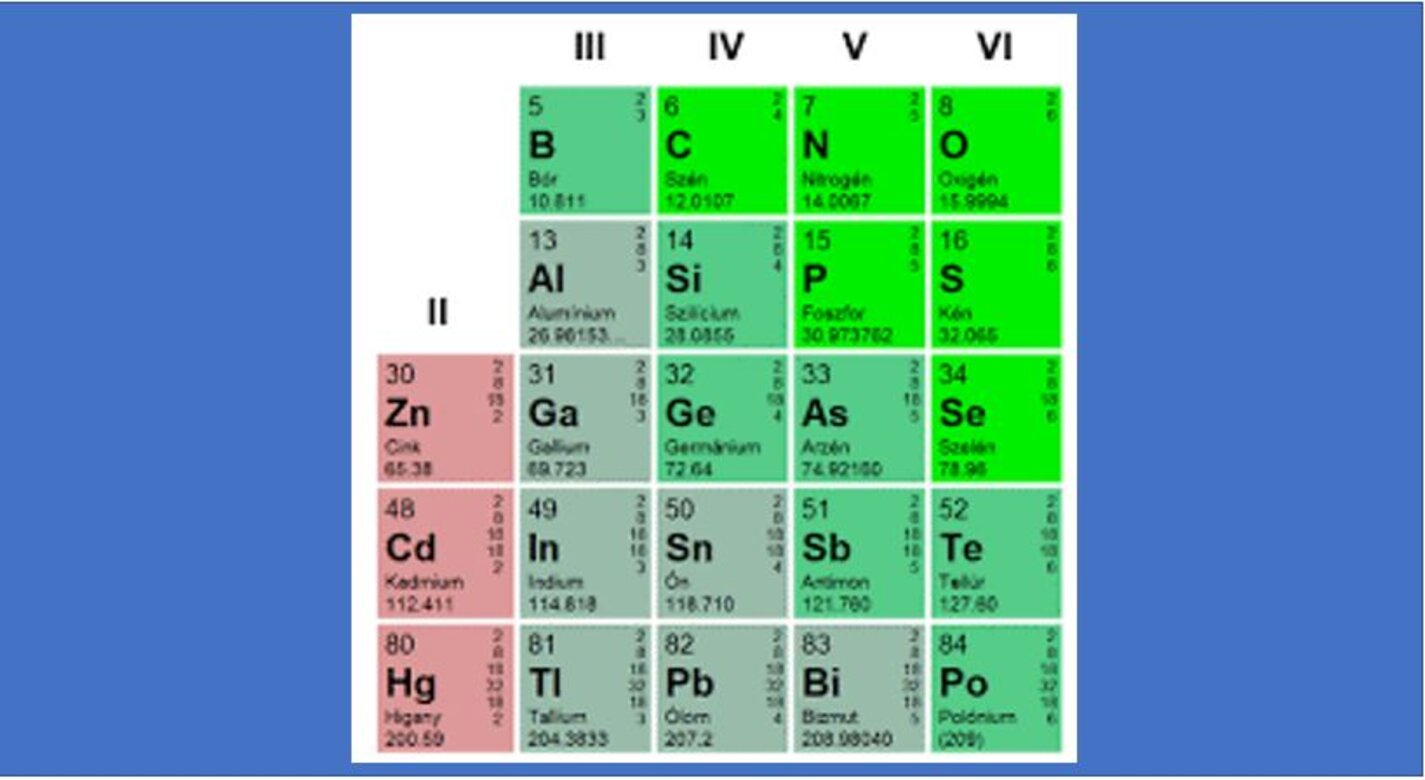
NASA engineers have developed a suite of technologies that enable super-hetero-epitaxial growth of silicon germanium (SiGe) and other compound semiconductors on sapphire and other trigonal and hexagonal structure substrate wafer materials. A focus for NASA has been on the development of methods to make SiGe crystal materials for the manufacture of advanced semiconductor devices for aerospace applications. This suite of technologies, however, is even more broadly applicable to making various semiconductors of Group IV, III-V, and II-VI compounds. The technologies include super-hetero-epitaxial growth using carefully engineered crystal structures/orientations combined with sputtering and control substrate heating. Also included are novel x-ray diffraction methods for detecting and mapping crystal twin defects that can arise during super-hetero-epitaxial growth. The specific case of growing highly twinned SiGe crystal layer structures for use in making high temperature thermoelectric devices is enabled as well.
The Technology
Several of the patented methods included in this suite of technologies enable super-hetero-epitaxy of rhombohedral/cubic compound semiconductors on specially oriented trigonal (e.g. sapphire) or hexagonal (e.g. quartz) crystal wafer substrates. This includes alignment of the growth crystal lattice with the underlying substrate lattice to minimize misfit strain-induced dislocation defects in the growing crystal. Thus thicker, defect-free crystal layers can be made. Rhombohedral/Cubic crystal twin defects which is 60 degree rotated on [111] orientation in a rhombohedral/cubic SiGe layer structure can be reduced to well less than 1% by volume, essentially providing a defect-free semiconductor material. Alternately, engineered lattice structures with a high degree of twinning can provide SiGe with improved thermoelectric properties due to the phonon scattering that inhibits thermal conduction without compromising electrical conductivity. Additional patented technologies in this suite provide for physical vapor deposition (PVD) growth methods utilizing molten sputtering targets and thermal control of heated substrates, including electron beam heating, in order to give the atoms in the sputtered vapor or on the substrate surface the energy needed for the desired crystal growth.
The remaining patented technologies enable x-ray diffraction methods for detecting and mapping crystal twin defects across the entire as-grown semiconductor layer. These defects are critical to the performance of any semiconductor device manufactured from such compound semiconductor materials.


Benefits
- Widely enabling: Suite of patented technologies enabling the manufacture of high-quality compound semiconductors on a variety of trigonal and hexagonal structured substrates.
- High-quality, defect-free: SiGe crystals grown on sapphire substrates, as a particular focus of these innovations, can be used to manufacture a number of advanced high performance semiconductor devices.
- Innovative processing: Physical vapor deposition (sputtering) of high-quality crystal structures is provided by selected crystal structure alignment coupled with energetic atomic transport and surface crystal arrangement (via high-temperature molten sputtering targets and controlled substrate heating).
- Innovative characterization: X-ray diffraction methods for detecting and mapping crystal twin defects in the as-grown semiconductor crystal material.
- New applications: Novel high temperature thermoelectric devices based on SiGe with highly twinned lattice structures, which reduce thermal conductivity without compromising electrical conductivity.
- Practical: Uses readily available materials, equipment and processes.
Applications
- This suite of technologies can be used to manufacture a range of novel, high-performance semiconductor devices like bipolar and high-mobility transistors. Additionally, novel photovoltaic, LED, phase shifter, power IC chips, RGB LEDs and thermoelectrics devices can be developed and manufactured using these methods. These high-performance devices can be used in various aerospace, industrial and consumer applications, including for extreme environments.
Technology Details
Materials and Coatings
LAR-TOPS-373
LAR-18574-1
LAR-18730-1
LAR-17044-1
LAR-17185-1
LAR-17381-1
LAR-17554-1
LAR-17553-1
LAR-18730-2
|
Tags:
|
Similar Results

Double Sided Si(Ge)/Sapphire/III-Nitride Hybrid Structures
III-nitride devices are commonly made on sapphire substrates today for various commercial electronic and optoelectronic applications. Thus, this innovation relates directly to the combination of devices on opposite sides of the sapphire substrate. One possible device combination is to have LEDs one side and solar cells on the other, such as for displays.

Single Crystal SiGe/Sapphire Epitaxy
This innovation is based on a new fabrication method that alleviates the thermal loading requirement of the substrate, which previously required surface temperatures within the range of 850 to 900C. Our method employs a new thermal loading requirement of sapphire substrate for growing single crystal SiGe on sapphire substrate, in the range of 450 to 500C. SiGe/sapphire wafers produced via this process show a high reflectivity without the discoloration that appears in low quality films.

High Mobility Transport Layer Structures for Rhombohedral Si/Ge/SiGe Devices
Performance of solar cells and other electronic devices such as transistors can be improved greatly if carrier mobility is increased. Si and Ge have Type-II bandgap alignment in cubically strained and relaxed layers. Quantum well and super lattice with Si, Ge, and SiGe have been good noble structures to build high electron mobility layer and high hole mobility layers. However, the atomic lattice constant of Ge is bigger than that of Si and direct epitaxial growth generates large density of misfit dislocations which decrease carrier mobility and shorten device life time. So it required special buffer layers such as super lattice or gradient indexed layers to grow Ge on Si wafers or Si on Ge wafers. The growth of these buffer layers takes extra effort and time such as post-annealing process to remove dislocations by dislocation gliding inside buffer layer.
This invention is a fabrication method for high mobility layer structures of rhombohedrally aligned SiGe on a trigonal substrate. The invention utilizes C-plane (0001) Sapphire which has a triangle plane, and a Si (Ge) (C) (111) crystal or an alloy of group TV semiconductor (111) crystal grown on the Sapphire.

Single Crystal Semiconductor Silicon-Germanium (SiGe)
Single Crystal SiGe semiconductors are viable via numerous advances patented by NASA. This includes the addition of a 1-2mm ring groove in the magnetron magnets which increases sputtering energy at 500C vs 800C, enabling thicker, faster deposition with better surface finish and consistent quality without heat soaking. The lack of thermal gradient removes inconsistencies in the product. SiGe can also utilize the CMOS manufacturing technique for additional cost savings and waste reduction.
Further decreases to time investment for single crystal SiGe is made possible via reduced thermal load and soak temperatures, growing SiGe semiconductors on, conveniently, less expensive sapphire substrates. Crystal lattice matched growing methods to the sapphire substrate ensure defect-free SiGe production without interfacial dislocations.
A graded indexed SiGe layer can be added to wafers grown in this lattice matched method, permitting thicker semiconductor growth without abrupt changes in strain build-up, carrier potential barrier, index of refraction change and bandgap at the interface. These advances provide improved semiconductor performance and quality with fewer defects in fabrication. The crystal alignment enables X-Ray diffraction identification of any defect location and density.
It is also possible to also grow a Gallium Nitride or Indium Gallium Nitride layer on the opposite side of the Sapphire wafer, useful for solar capable LED display.
A type II band-gap alignment of SiGe would result in highly efficient solar cells – attaining 30% to 40% energy conversion efficiency.
In addition to SiGe, the patented technology also covers these methodologies on tin-based or carbon-based semiconductors.

Integrated Circuit Chips
NASA Glenn's durable, extreme-temperature, integrated circuit chips begin with the replacement of conventional silicon IC transistors with n-channel SiC junction field effect transistors (JFET) and resistors that can reliably function above 500°C. JFETs with the necessary high-temperature stability and electrical gain are fabricated from commercial 4H-SiC wafers with epilayers using dry etching and a self-aligned n-type ion implantation. An innovative circuit approach creates digital logic gates from these normally-on n-channel JFETs and resistors. Using two levels of 500°C durable metal to interconnect numerous SiC gates, complex circuits enabling a variety of control, operation and sensing functions for intelligent systems in harsh environments can be implemented in physically small chips. The challenge of getting electrical signals to and from the chip in a harsh environment is overcome by the use of the iridium interfacial stack (IrIS) that acts simultaneously as a bond metal and diffusion barrier, and can be used on an ohmic contact to the SiC. Combined with Glenn-developed high-temperature durable ceramic chip packaging and harsh environment sensor technology, this revolutionary durable integrated circuit technology is game changing for harsh-environment applications of all types.


