High Mobility Transport Layer Structures for Rhombohedral Si/Ge/SiGe Devices
electrical and electronics
High Mobility Transport Layer Structures for Rhombohedral Si/Ge/SiGe Devices (LAR-TOPS-166)
Improved carrier mobility for solar cells and other electronic devices
Overview
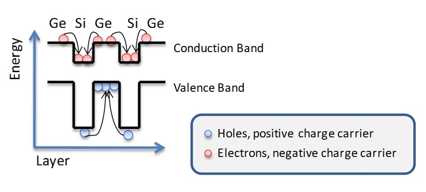
The innovation builds off NASA's IP portfolio for making high-quality crystalline SiGe thin films grown on sapphire substrates. In this case, a distinct layer structure is used to create quantum well structures to provide a very high mobility pathway for both p-type and n-type charge carriers. The primary intended application of this technology is for solar cells where the band gap structure and charge carrier mobility combine to provide the potential for highly efficient solar cells. Furthermore the layer structure enables back-side illumination such that the effective solar cell area for light capture is maximized. Conversion efficiency is expected to be on the order of 30% or greater.
The Technology
Performance of solar cells and other electronic devices such as transistors can be improved greatly if carrier mobility is increased. Si and Ge have Type-II bandgap alignment in cubically strained and relaxed layers. Quantum well and super lattice with Si, Ge, and SiGe have been good noble structures to build high electron mobility layer and high hole mobility layers. However, the atomic lattice constant of Ge is bigger than that of Si and direct epitaxial growth generates large density of misfit dislocations which decrease carrier mobility and shorten device life time. So it required special buffer layers such as super lattice or gradient indexed layers to grow Ge on Si wafers or Si on Ge wafers. The growth of these buffer layers takes extra effort and time such as post-annealing process to remove dislocations by dislocation gliding inside buffer layer.
This invention is a fabrication method for high mobility layer structures of rhombohedrally aligned SiGe on a trigonal substrate. The invention utilizes C-plane (0001) Sapphire which has a triangle plane, and a Si (Ge) (C) (111) crystal or an alloy of group TV semiconductor (111) crystal grown on the Sapphire.


Benefits
- Potential for high-efficiency thin film solar cells, 30% conversion efficiency or greater
- Uses conventional thin film processes commonly used in silicon semiconductor processing
- Materials are relatively abundant, low-cost, and non-toxic as compared to other leading thin film solar cell materials
- Backside illumination reduces solar radiation losses from electrical contacts
Applications
- Solar cells
- Semiconductors
- Thermo-electric devices
Technology Details
electrical and electronics
LAR-TOPS-166
LAR-17841-1
LAR-17841-2
Similar Results

Single Crystal Semiconductor Silicon-Germanium (SiGe)
Single Crystal SiGe semiconductors are viable via numerous advances patented by NASA. This includes the addition of a 1-2mm ring groove in the magnetron magnets which increases sputtering energy at 500C vs 800C, enabling thicker, faster deposition with better surface finish and consistent quality without heat soaking. The lack of thermal gradient removes inconsistencies in the product. SiGe can also utilize the CMOS manufacturing technique for additional cost savings and waste reduction.
Further decreases to time investment for single crystal SiGe is made possible via reduced thermal load and soak temperatures, growing SiGe semiconductors on, conveniently, less expensive sapphire substrates. Crystal lattice matched growing methods to the sapphire substrate ensure defect-free SiGe production without interfacial dislocations.
A graded indexed SiGe layer can be added to wafers grown in this lattice matched method, permitting thicker semiconductor growth without abrupt changes in strain build-up, carrier potential barrier, index of refraction change and bandgap at the interface. These advances provide improved semiconductor performance and quality with fewer defects in fabrication. The crystal alignment enables X-Ray diffraction identification of any defect location and density.
It is also possible to also grow a Gallium Nitride or Indium Gallium Nitride layer on the opposite side of the Sapphire wafer, useful for solar capable LED display.
A type II band-gap alignment of SiGe would result in highly efficient solar cells – attaining 30% to 40% energy conversion efficiency.
In addition to SiGe, the patented technology also covers these methodologies on tin-based or carbon-based semiconductors.

High-Efficiency Solar Cell
This NASA Glenn innovation is a novel multi-junction photovoltaic cell constructed using selenium as a bonding material sandwiched between a thin film multi-junction wafer and a silicon substrate wafer, enabling higher efficiencies. A multi-junction photovoltaic cell differs from a single junction cell in that it has multiple sub-cells (p-n junctions) and can convert more of the sun's energy into electricity as the light passes through each layer. To further improve the efficiencies, this cell has three junctions, where the top wafer is made from high solar energy absorbing materials that form a two-junction cell made from the III-V semiconductor family, and the bottom substrate remains as a simple silicon wafer. The selenium interlayer is applied between the top and bottom wafers, then pressure annealed at 221°C (the melting temperature of selenium), then cooled. The selenium interlayer acts as a connective layer between the top cell that absorbs the short-wavelength light and the bottom silicon-based cell that absorbs the longer wavelengths. The three-junction solar cell manufactured using selenium as the transparent interlayer has a higher efficiency, converting more than twice the energy into electricity than traditional cells. To obtain even higher efficiencies of over 40%, both the top and bottom layers can be multi-junction solar cells with the selenium layer sandwiched in between. The resultant high performance multi-junction photovoltaic cell with the selenium interlayer provides more power per unit area while utilizing a low-cost silicon-based substrate. This unprecedented combination of increased efficiency and cost savings has considerable commercial potential.
This is an early-stage technology requiring additional development. Glenn welcomes co-development opportunities.

Epitaxy of SiGe and Other Compound Semiconductors
Several of the patented methods included in this suite of technologies enable super-hetero-epitaxy of rhombohedral/cubic compound semiconductors on specially oriented trigonal (e.g. sapphire) or hexagonal (e.g. quartz) crystal wafer substrates. This includes alignment of the growth crystal lattice with the underlying substrate lattice to minimize misfit strain-induced dislocation defects in the growing crystal. Thus thicker, defect-free crystal layers can be made. Rhombohedral/Cubic crystal twin defects which is 60 degree rotated on [111] orientation in a rhombohedral/cubic SiGe layer structure can be reduced to well less than 1% by volume, essentially providing a defect-free semiconductor material. Alternately, engineered lattice structures with a high degree of twinning can provide SiGe with improved thermoelectric properties due to the phonon scattering that inhibits thermal conduction without compromising electrical conductivity. Additional patented technologies in this suite provide for physical vapor deposition (PVD) growth methods utilizing molten sputtering targets and thermal control of heated substrates, including electron beam heating, in order to give the atoms in the sputtered vapor or on the substrate surface the energy needed for the desired crystal growth.
The remaining patented technologies enable x-ray diffraction methods for detecting and mapping crystal twin defects across the entire as-grown semiconductor layer. These defects are critical to the performance of any semiconductor device manufactured from such compound semiconductor materials.

Single Crystal SiGe/Sapphire Epitaxy
This innovation is based on a new fabrication method that alleviates the thermal loading requirement of the substrate, which previously required surface temperatures within the range of 850 to 900C. Our method employs a new thermal loading requirement of sapphire substrate for growing single crystal SiGe on sapphire substrate, in the range of 450 to 500C. SiGe/sapphire wafers produced via this process show a high reflectivity without the discoloration that appears in low quality films.

Double Sided Si(Ge)/Sapphire/III-Nitride Hybrid Structures
III-nitride devices are commonly made on sapphire substrates today for various commercial electronic and optoelectronic applications. Thus, this innovation relates directly to the combination of devices on opposite sides of the sapphire substrate. One possible device combination is to have LEDs one side and solar cells on the other, such as for displays.


