Search

manufacturing
Microchips
X-Ray Diffraction Method to Detect Defects in Cubic Semiconductor (100) Wafers
This technology is a method of using x-ray diffraction (XRD) to evaluate the concentration of crystal structure defects, and thus the quality, of cubic (100)-oriented semiconductor wafers. Developed to enhance NASA's capabilities in fabricating chips for aeronautics applications, the method supplants existing methods that not only destroy the wafer in question, but can take as long as a day to determine the quality of a single wafer. The approach can be used with any commonly used semiconductor, including silicon, SiGe, GaAs and others, in a cubic (100) orientation, which covers at least 90% of commercial wafers. It can also be used to evaluate the quality of epi layers deposited on wafer substrates, and of ingots before they are sliced into wafers.
electrical and electronics
Tablet computer in the sun
Double Sided Si(Ge)/Sapphire/III-Nitride Hybrid Structures
III-nitride devices are commonly made on sapphire substrates today for various commercial electronic and optoelectronic applications. Thus, this innovation relates directly to the combination of devices on opposite sides of the sapphire substrate. One possible device combination is to have LEDs one side and solar cells on the other, such as for displays.
electrical and electronics
Solar panels on rooftop
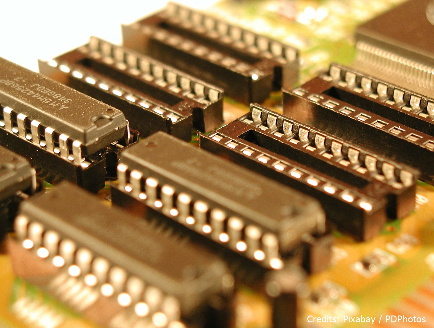
High Mobility Transport Layer Structures for Rhombohedral Si/Ge/SiGe Devices
Performance of solar cells and other electronic devices such as transistors can be improved greatly if carrier mobility is increased. Si and Ge have Type-II bandgap alignment in cubically strained and relaxed layers. Quantum well and super lattice with Si, Ge, and SiGe have been good noble structures to build high electron mobility layer and high hole mobility layers. However, the atomic lattice constant of Ge is bigger than that of Si and direct epitaxial growth generates large density of misfit dislocations which decrease carrier mobility and shorten device life time. So it required special buffer layers such as super lattice or gradient indexed layers to grow Ge on Si wafers or Si on Ge wafers. The growth of these buffer layers takes extra effort and time such as post-annealing process to remove dislocations by dislocation gliding inside buffer layer. This invention is a fabrication method for high mobility layer structures of rhombohedrally aligned SiGe on a trigonal substrate. The invention utilizes C-plane (0001) Sapphire which has a triangle plane, and a Si (Ge) (C) (111) crystal or an alloy of group TV semiconductor (111) crystal grown on the Sapphire.
optics
MIDAR
Multispectral Imaging, Detection, and Active Reflectance (MiDAR)
The MiDAR transmitter emits coded narrowband structured illumination to generate high-frame-rate multispectral video, perform real-time radiometric calibration, and provide a high-bandwidth simplex optical data-link under a range of ambient irradiance conditions, including darkness. A theoretical framework, based on unique color band signatures, is developed for multispectral video reconstruction and optical communications algorithms used on MiDAR transmitters and receivers. Experimental tests demonstrate a 7-channel MiDAR prototype consisting of an active array of multispectral high-intensity light-emitting diodes (MiDAR transmitter) coupled with a state-of-the-art, high-frame-rate NIR computational imager, the NASA FluidCam NIR, which functions as a MiDAR receiver. A 32-channel instrument is currently in development. Preliminary results confirm efficient, radiometrically-calibrated, high signal-to-noise ratio (SNR) active multispectral imaging in 7 channels from 405-940 nm at 2048x2048 pixels and 30 Hz. These results demonstrate a cost-effective and adaptive sensing modality, with the ability to change color bands and relative intensities in real-time, in response to changing science requirements or dynamic scenes. Potential applications of MiDAR include high-resolution nocturnal and diurnal multispectral imaging from air, space and underwater environments as well as long- distance optical communication, bidirectional reflectance distribution function characterization, mineral identification, atmospheric correction, UV/fluorescent imaging, 3D reconstruction using Structure from Motion (SfM), and underwater imaging using Fluid Lensing. Multipurpose sensors, such as MiDAR, which fuse active sensing and communications capabilities, may be particularly well-suited for mass-limited robotic exploration of Earth and the solar system and represent a possible new generation of instruments for active optical remote sensing.
manufacturing
Atmospheric Pressure Plasma Based Fabrication of Printable Electronics and Functional Coatings
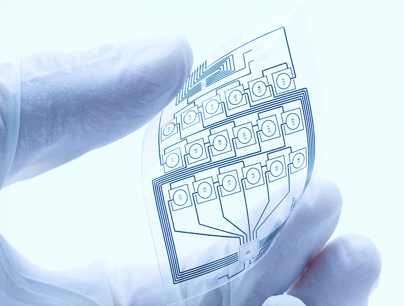
Fabricating printable electronics and biosensor chips
The plasma system consists of a glass tube with a diameter of 0.5 mm or larger, if desired. The electrodes are separated by 10 mm. Helium, argon or cold dry air can be used as a plasma gas source. An applied high voltage between the electrodes causes the gas to breakdown within the central core of the glass capillary generating atmospheric plasma. Nanostructures colloids/organic/inorganic precursors are placed in a glass container with an inlet and outlet for carrier gas and are seated on an ultrasonic nebuliser. The aerosol is then carried into the plasma stream by the carrier gas and is deposited. The atmospheric plasma deposition system can be modified for depositing multiple materials, either simultaneously or sequentially, and for high-throughput processing by having multiple jets. Each capillary can either be connected to the container containing a single precursor material or to different containers containing different precursor materials to facilitate multiple depositions. The multi-jet plasma system can be automated and controlled individually to precisely control surface characteristics. This technique is independent of the chosen substrate, and has proven to work for many substrates, including paper, plastic, semiconductors and metals.
instrumentation
3D Laser Scanner
ShuttleSCAN 3-D
How It Works The scanners operation is based on the principle of Laser Triagulation. The ShuttleSCAN contains an imaging sensor; two lasers mounted on opposite sides of the imaging sensor; and a customized, on-board processor for processing the data from the imaging sensor. The lasers are oriented at a given angle and surface height based on the size of objects being examined. For inspecting small details, such as defects in space shuttle tiles, a scanner is positioned close to the surface. This creates a small field of view but with very high resolution. For scanning larger objects, such as use in a robotic vision application, a scanner can be positioned several feet above the surface. This increases the field of view but results in slightly lower resolution. The laser projects a line on the surface, directly below the imaging sensor. For a perfectly flat surface, this projected line will be straight. As the ShuttleSCAN head moves over the surface, defects or irregularities above and below the surface will cause the line to deviate from perfectly straight. The SPACE processors proprietary algorithms interpret these deviations in real time and build a representation of the defect that is then transmitted to an attached PC for triangulation and 3-D display or printing. Real-time volume calculation of the defect is a capability unique to the ShuttleSCAN system. Why It Is Better The benefits of the ShuttleSCAN 3-D system are very unique in the industry. No other 3-D scanner can offer the combination of speed, resolution, size, power efficiency, and versatility. In addition, ShuttleSCAN can be used as a wireless instrument, unencumbered by cables. Traditional scanning systems make a tradeoff between resolution and speed. ShuttleSCANs onboard SPACE processor eliminates this tradeoff. The system scans at speeds greater than 600,000 points per second, with a resolution smaller than .001". Results of the scan are available in real time, whereas conventional systems scan over the surface, analyze the scanned data, and display the results long after the scan is complete.
Stay up to date, follow NASA's Technology Transfer Program on:
facebook twitter linkedin youtube
Facebook Logo Twitter Logo Linkedin Logo Youtube Logo