Search
sensors
Room temperature oxygen sensors
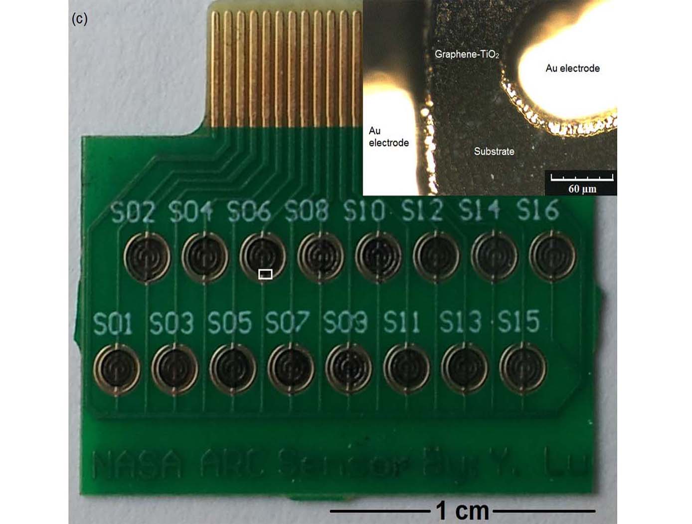
NASA Ames has developed very small-sized oxygen sensors made of a graphene and titanium dioxide (TiO<sub>2</sub>) hybrid material. With ultraviolet (UV) illumination, these sensors are capable of detecting oxygen (O<sub>2</sub>) gas at room temperature and at ambient pressure. The sensors are able to detect oxygen at concentrations ranging from about 0.2% to about 10% by volume under 365nm UV light, and at concentrations ranging from 0.4% to 20% by volume under short wave 254nm UV light. These sensors have fast response and recovery times and can also be used to detect ozone.
This unique room temperature O<sub>2</sub> sensor provides significant advantages in O<sub>2</sub> sensing applications, especially those applications where high operating temperature requirements cannot be met, or would result in inefficient manufacturing processes. Since graphene is not intrinsically responsive to O<sub>2</sub>, and TiO<sub>2</sub> is not responsive to oxygen at room temperature, the materials are first synthesized as a hybrid material. The synthesized graphene- TiO<sub>2</sub> hybrid material is then ultrasonicated and then drop-casted onto a series of Interdigitated Electrodes (IDE) to form the sensors.
Ultrasonication ensures effective charge transfer at the graphene- TiO<sub>2</sub> interphase. The graphene and the titanium dioxide may be present in the composite material in different ratios to ensure optimal oxygen detection. It is the combination of graphene with TiO2 that yields a semiconducting material capable of O<sub>2</sub> sensing at room-temperature operation.
Materials and Coatings
Epitaxy of SiGe and Other Compound Semiconductors
Several of the patented methods included in this suite of technologies enable super-hetero-epitaxy of rhombohedral/cubic compound semiconductors on specially oriented trigonal (e.g. sapphire) or hexagonal (e.g. quartz) crystal wafer substrates. This includes alignment of the growth crystal lattice with the underlying substrate lattice to minimize misfit strain-induced dislocation defects in the growing crystal. Thus thicker, defect-free crystal layers can be made. Rhombohedral/Cubic crystal twin defects which is 60 degree rotated on [111] orientation in a rhombohedral/cubic SiGe layer structure can be reduced to well less than 1% by volume, essentially providing a defect-free semiconductor material. Alternately, engineered lattice structures with a high degree of twinning can provide SiGe with improved thermoelectric properties due to the phonon scattering that inhibits thermal conduction without compromising electrical conductivity. Additional patented technologies in this suite provide for physical vapor deposition (PVD) growth methods utilizing molten sputtering targets and thermal control of heated substrates, including electron beam heating, in order to give the atoms in the sputtered vapor or on the substrate surface the energy needed for the desired crystal growth.
The remaining patented technologies enable x-ray diffraction methods for detecting and mapping crystal twin defects across the entire as-grown semiconductor layer. These defects are critical to the performance of any semiconductor device manufactured from such compound semiconductor materials.

