Search
Manufacturing
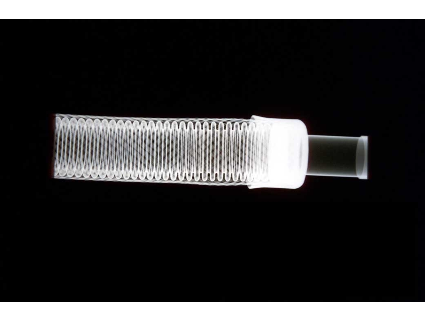
X-Ray Crack Detectability
NASAs software technology uses an Image Quality Indicator (IQI)-based model that can predict whether cracks of a certain size can be detected, as well as a model that can provide appropriate conditions to optimize x-ray crack detection setup. Because this modeling software can predict minimum crack sizes that can be detected by a particular X-ray radiography testing setup, users can test various setups until the desired crack detection capabilities are achieved (predicted) by the modeling system.
These flaw size parameter models use a set of measured inputs, including thickness sensitivity, detector modulation transfer function, detector signal response function, and other setup geometry parameters, to predict the minimum crack sizes detectable by the testing setup and X-ray angle limits for detecting such flaws.
Current X-ray methods provide adequate control for detection of volumetric flaws but do not provide a high probability of detection (POD), and crack detection sensitivity cannot be verified for reliable detection. This results in reduced confidence in terms of crack detection. Given that these cracks, if undetected, can cause catastrophic failure in various systems (e.g., pressure vessels, etc.), verifying that X-ray radiography systems used for NDE can detect such cracks is of the utmost importance in many applications.
Manufacturing

Optimization of X-Ray CT Measurement Accuracy for Metal AM Components
This NASA innovation is a method for quantifying and improving accuracy of X-Ray CT-based metal AM part inspection by comparing X-Ray CT data with a high-fidelity 2D surface imaging technique such as surface profilometry. Using surface profilometry that has a NIST-traceable calibration, the technique guarantees a specific level of high fidelity, allowing surface profilometry data to serve as a ground truth reference with which to judge X-Ray CT accuracy and detectability.
To deploy the method, both 3D X-Ray CT data and 2D high-fidelity surface images are acquired on the same metal AM part. 3D X-Ray CT data is then segmented and reoriented to extract a 2D X-Ray CT surface image. Measurements of features (e.g., surface-breaking porosity) are then made in both datasets, followed by a comparison of various metrics. This comparison serves two purposes: (a) quantifying the accuracy of the X-Ray CT inspection performed, and (b) providing an objective function which can be minimized to optimize X-Ray CT inspection. The objective function allows engineers to tune X-Ray CT parameters to minimize the function. These optimized parameters can then be implemented to achieve higher accuracy and defect detection reliability in X-Ray CT imaging. Once an X-Ray CT process is optimized for a specific metal AM component, analysis and certification can be accelerated.
This technology helps develop X-Ray CT-based metal AM part inspection processes with high accuracy and reliable detectability. Industries for which metal AM parts are desirable and safety, reliability, and fatigue life is of concern (e.g., aerospace, commercial space, automotive, medical) could benefit from the invention. Companies including X-Ray CT inspection system manufacturers using optical sensors and software, NDE data analysis software providers, and end-users in the industries may be interested in licensing this NASA invention.
Materials and Coatings
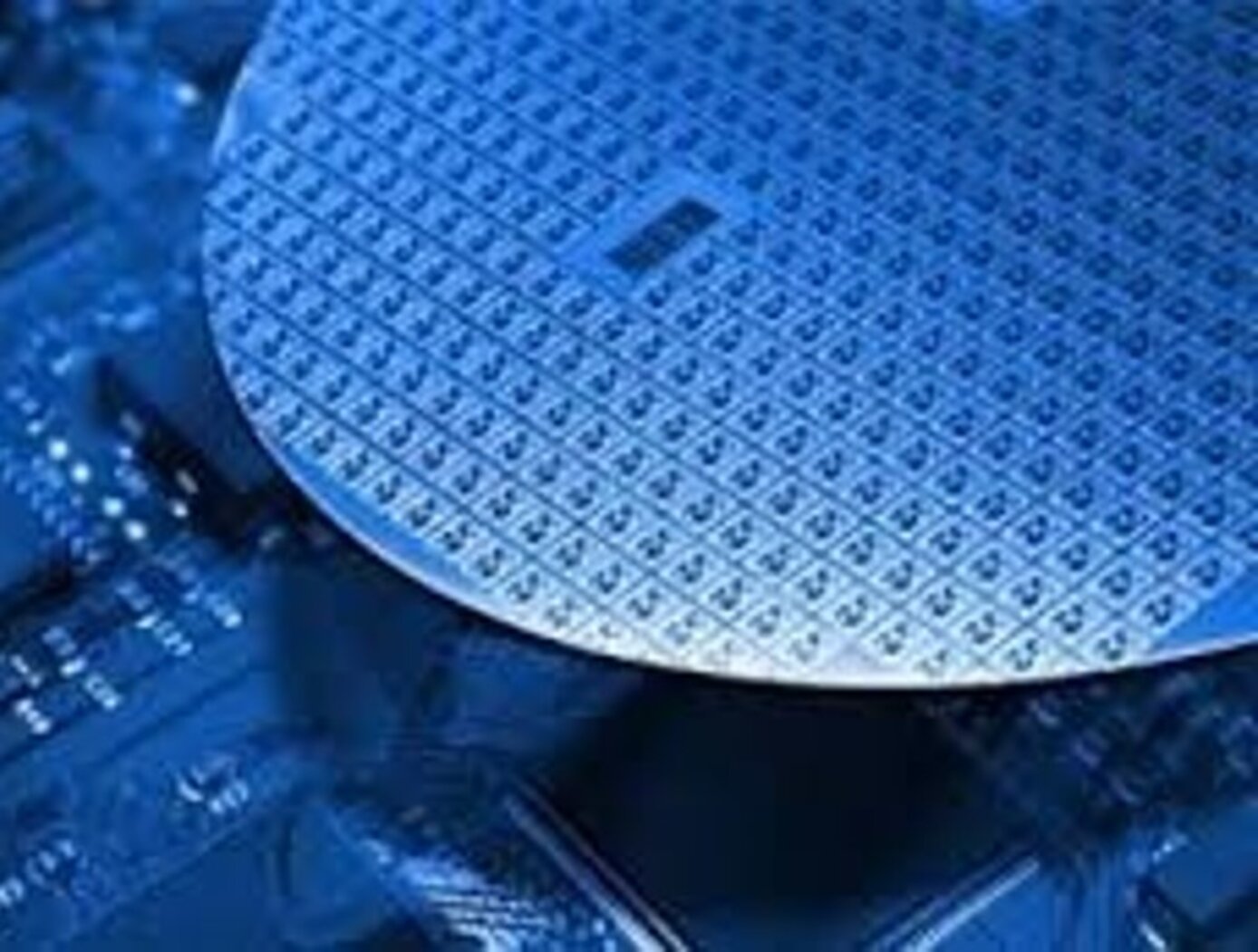
Epitaxy of SiGe and Other Compound Semiconductors
Several of the patented methods included in this suite of technologies enable super-hetero-epitaxy of rhombohedral/cubic compound semiconductors on specially oriented trigonal (e.g. sapphire) or hexagonal (e.g. quartz) crystal wafer substrates. This includes alignment of the growth crystal lattice with the underlying substrate lattice to minimize misfit strain-induced dislocation defects in the growing crystal. Thus thicker, defect-free crystal layers can be made. Rhombohedral/Cubic crystal twin defects which is 60 degree rotated on [111] orientation in a rhombohedral/cubic SiGe layer structure can be reduced to well less than 1% by volume, essentially providing a defect-free semiconductor material. Alternately, engineered lattice structures with a high degree of twinning can provide SiGe with improved thermoelectric properties due to the phonon scattering that inhibits thermal conduction without compromising electrical conductivity. Additional patented technologies in this suite provide for physical vapor deposition (PVD) growth methods utilizing molten sputtering targets and thermal control of heated substrates, including electron beam heating, in order to give the atoms in the sputtered vapor or on the substrate surface the energy needed for the desired crystal growth.
The remaining patented technologies enable x-ray diffraction methods for detecting and mapping crystal twin defects across the entire as-grown semiconductor layer. These defects are critical to the performance of any semiconductor device manufactured from such compound semiconductor materials.

