X-Ray Crack Detectability
Manufacturing
X-Ray Crack Detectability (MSC-TOPS-106)
Optimizes X-ray radiography setups for crack sensitivity verification
Overview
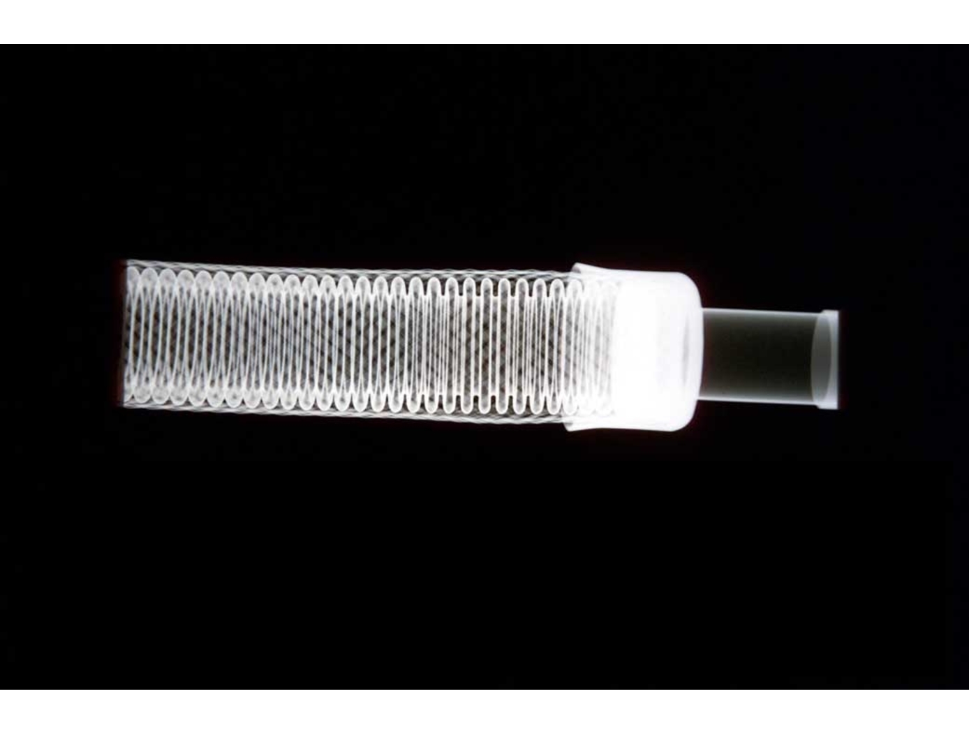
Innovators at NASA Johnson Space Center have developed flaw size parameter modeling to determine if a specific X-ray setup can detect cracks of various sizes within materials. These models allow users to optimize X-ray radiography setups, for the detection of crack and crack-like flaws, to penetrate various materials to show internal structures such as the threaded pipe shown above.
The ability to quantify crack detection sensitivity paves the way for crack detection requirements to be defined for X-ray radiography nondestructive evaluation (NDE) of manufactured parts. Improved industry requirements for reliable crack detection using x-ray radiography and improved X-ray setup optimization tools that are based on software modeling, such as this technology, may be desired by industry.
The Model-Based X-Ray Crack Detection Requirements is a technology readiness level (TRL) 6 (system/sub-system model or prototype demonstrated in an operational environment). The innovation is now available for your company to license. Please note that NASA does not manufacture products itself for commercial sale.
The Technology
NASAs software technology uses an Image Quality Indicator (IQI)-based model that can predict whether cracks of a certain size can be detected, as well as a model that can provide appropriate conditions to optimize x-ray crack detection setup. Because this modeling software can predict minimum crack sizes that can be detected by a particular X-ray radiography testing setup, users can test various setups until the desired crack detection capabilities are achieved (predicted) by the modeling system.
These flaw size parameter models use a set of measured inputs, including thickness sensitivity, detector modulation transfer function, detector signal response function, and other setup geometry parameters, to predict the minimum crack sizes detectable by the testing setup and X-ray angle limits for detecting such flaws.
Current X-ray methods provide adequate control for detection of volumetric flaws but do not provide a high probability of detection (POD), and crack detection sensitivity cannot be verified for reliable detection. This results in reduced confidence in terms of crack detection. Given that these cracks, if undetected, can cause catastrophic failure in various systems (e.g., pressure vessels, etc.), verifying that X-ray radiography systems used for NDE can detect such cracks is of the utmost importance in many applications.

Benefits
- Characterizes crack detection capabilities
- Optimizes and verifies X-ray radiography test setups
- Uses non-invasive procedure on test article
- Provides high probability of detection
- Enables establishment of crack detection requirements/standards for enhanced quality control
- Inexpensive to operate
Applications
- Aerospace
- Automotive
- Civil engineering
- Gas and oil pipeline manufacturing
- Gas turbine manufacturing
- Industrial manufacturing
- Maritime vessels
- Medical implant and prosthetic manufacturing
- Structural engineering
Similar Results

X-Ray Diffraction Method to Detect Defects in Cubic Semiconductor (100) Wafers
This technology is a method of using x-ray diffraction (XRD) to evaluate the concentration of crystal structure defects, and thus the quality, of cubic (100)-oriented semiconductor wafers. Developed to enhance NASA's capabilities in fabricating chips for aeronautics applications, the method supplants existing methods that not only destroy the wafer in question, but can take as long as a day to determine the quality of a single wafer. The approach can be used with any commonly used semiconductor, including silicon, SiGe, GaAs and others, in a cubic (100) orientation, which covers at least 90% of commercial wafers. It can also be used to evaluate the quality of epi layers deposited on wafer substrates, and of ingots before they are sliced into wafers.

Optimization of X-Ray CT Measurement Accuracy for Metal AM Components
This NASA innovation is a method for quantifying and improving accuracy of X-Ray CT-based metal AM part inspection by comparing X-Ray CT data with a high-fidelity 2D surface imaging technique such as surface profilometry. Using surface profilometry that has a NIST-traceable calibration, the technique guarantees a specific level of high fidelity, allowing surface profilometry data to serve as a ground truth reference with which to judge X-Ray CT accuracy and detectability.
To deploy the method, both 3D X-Ray CT data and 2D high-fidelity surface images are acquired on the same metal AM part. 3D X-Ray CT data is then segmented and reoriented to extract a 2D X-Ray CT surface image. Measurements of features (e.g., surface-breaking porosity) are then made in both datasets, followed by a comparison of various metrics. This comparison serves two purposes: (a) quantifying the accuracy of the X-Ray CT inspection performed, and (b) providing an objective function which can be minimized to optimize X-Ray CT inspection. The objective function allows engineers to tune X-Ray CT parameters to minimize the function. These optimized parameters can then be implemented to achieve higher accuracy and defect detection reliability in X-Ray CT imaging. Once an X-Ray CT process is optimized for a specific metal AM component, analysis and certification can be accelerated.
This technology helps develop X-Ray CT-based metal AM part inspection processes with high accuracy and reliable detectability. Industries for which metal AM parts are desirable and safety, reliability, and fatigue life is of concern (e.g., aerospace, commercial space, automotive, medical) could benefit from the invention. Companies including X-Ray CT inspection system manufacturers using optical sensors and software, NDE data analysis software providers, and end-users in the industries may be interested in licensing this NASA invention.

In-situ Characterization and Inspection of Additive Manufacturing Deposits using Transient Infrared Thermography
Additive manufacturing or 3-D printing is a rapidly growing field where solid, objects can be produced layer by layer. This technology will have a significant impact in many areas including industrial manufacturing, medical, architecture, aerospace, and automotive. The advantages of additive manufacturing are reduction in material costs due to near net shape part builds, minimal machining required, computer assisted builds for rapid prototyping, and mass production capability. Traditional thermal nondestructive evaluation (NDE) techniques typically use a stationary heat source such as flash or quartz lamp heating to induce a temperature rise. The defects such as cracks, delamination damage, or voids block the heat flow and therefore cause a change in the transient heat flow response. There are drawbacks to these methods.

System for In-situ Defect Detection in Composites During Cure
NASA's System for In-situ Defect (e.g., porosity, fiber waviness) Detection in Composites During Cure consists of an ultrasonic portable automated C-Scan system with an attached ultrasonic contact probe. This scanner is placed inside of an insulated vessel that protects the temperature-sensitive components of the scanner. A liquid nitrogen cooling systems keeps the interior of the vessel below 38°C. A motorized X-Y raster scanner is mounted inside an unsealed cooling container made of porous insulation boards with a cantilever scanning arm protruding out of the cooling container through a slot. The cooling container that houses the X-Y raster scanner is periodically cooled using a liquid nitrogen (LN2) delivery system. Flexible bellows in the slot opening of the box minimize heat transfer between the box and the external autoclave environment. The box and scanning arm are located on a precision cast tool plate. A thin layer of ultrasonic couplant is placed between the transducer and the tool plate. The composite parts are vacuum bagged on the other side of the tool plate and inspected. The scanning system inside of the vessel is connected to the controller outside of the autoclave. The system can provide A-scan, B-scan, and C-scan images of the composite panel at multiple times during the cure process.
The in-situ system provides higher resolution data to find, characterize, and track defects during cure better than other cure monitoring techniques. In addition, this system also shows the through-thickness location of any composite manufacturing defects during cure with real-time localization and tracking. This has been demonstrated for both intentionally introduced porosity (i.e., trapped during layup) as well processing induced porosity (e.g., resulting from uneven pressure distribution on a part). The technology can be used as a non-destructive evaluation system when making composite parts in in an oven or an autoclave, including thermosets, thermoplastics, composite laminates, high-temperature resins, and ceramics.
.jpg)
Interim, In Situ Additive Manufacturing Inspection
The in situ inspection technology for additive manufacturing combines different types of cameras strategically placed around the part to monitor its properties during construction. The IR cameras collect accurate temperature data to validate thermal math models, while the visual cameras obtain highly detailed data at the exact location of the laser to build accurate, as-built geometric models. Furthermore, certain adopted techniques (e.g., single to grouped pixels comparison to avoid bad/biased pixels) reduce false positive readings.
NASA has developed and tested prototypes in both laser-sintered plastic and metal processes. The technology detected errors due to stray powder sparking and material layer lifts. Furthermore, the technology has the potential to detect anomalies in the property profile that are caused by errors due to stress, power density issues, incomplete melting, voids, incomplete fill, and layer lift-up. Three-dimensional models of the printed parts were reconstructed using only the collected data, which demonstrates the success and potential of the technology to provide a deeper understanding of the laser-metal interactions. By monitoring the print, layer by layer, in real-time, users can pause the process and make corrections to the build as needed, reducing material, energy, and time wasted in nonconforming parts.

