Robust High Temperature SiC Op Amps Practical Fabrication
electrical and electronics
Robust High Temperature SiC Op Amps Practical Fabrication (LEW-TOPS-160)
Amplifiers with invariance to SiC transistor threshold voltage variations
Overview
NASA Glenn has a new way to correct for variations in transistor threshold voltage due to die location on the wafer for silicon carbide (SiC) op amps, enabling improved electrical circuits for sensor signal conditioning in harsh environments. Important system-level benefits are enabled by improved performance data from sensor circuitry mounted within very hot gas turbine flows or the primary coolant loop of a nuclear reactor, for example. Often, tiny (microvolt) signals from sensors require conditioning by high-temperature electrical components to filter, amplify and convert to levels suitable for digitization and "smart" system control. Op amps are a critical component for signal amplification. With the new threshold voltage correction scheme, the signal amplification of all op amps, at any position on the SiC wafer, is the same, extending reliable signal conditioning well beyond the current temperature limits of conventional silicon integrated circuits allowing useful chips to be produced across the entire SiC wafer surface.
The Technology
The technology is part of a new generation of NASA Glenn SiC integrated circuits with unprecedented durability in the field of high-temperature electronics. For robust operational amplifiers based on SiC Junction Field Effect Transistors (JFETs), this novel compensation method mitigates issues with threshold voltage variations that are an effect of die location on the wafer. Modern high-temperature op amps on the market fall short due to temperature limits (only 225C for silicon-based devices). Previously, researchers noted that multiple op amps on a single SiC wafer had different amplification properties due to different threshold voltages that varied spatially as much as 18% depending on the circuit's distance from the SiC wafer center. While 18% is okay for some applications, other important system applications demand better precision. By applying this technology to the amplifier circuit design process, the op amp will provide the same signal gain no matter its position on the wafer. The compensation approach enables practical signal conditioning that works from 25C up to 500C.
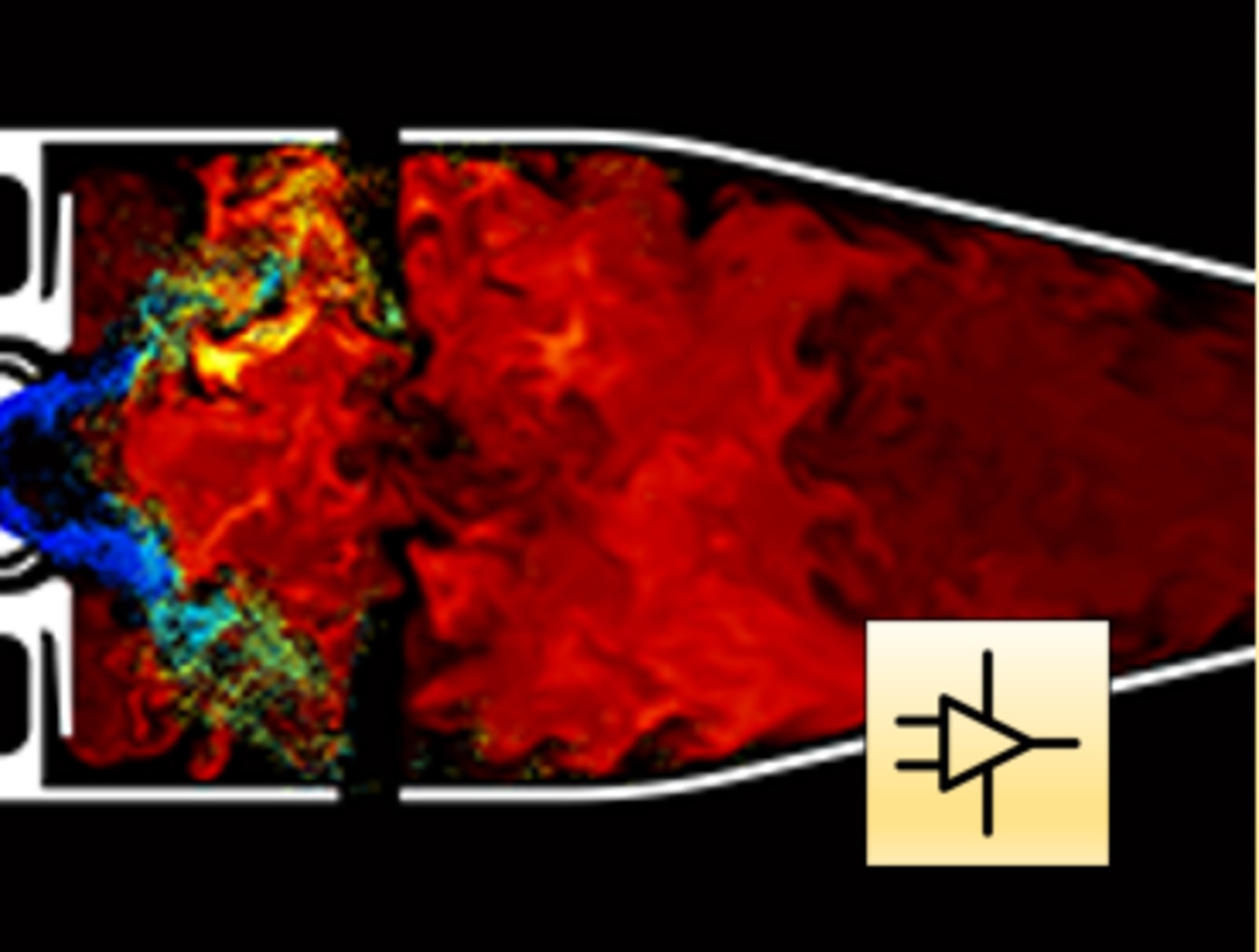
 and four output signal plots (red) for inverting amplifiers made from SiC op amps at different locations on the SiC wafer. The four output signal waveforms overlap each other, proving the identical signal amplification despite the difference in transistor threshold voltages with temperature and SiC wafer position. Note: the gain is set to -10 and the input sine wave has an amplitude of 50 mV peak.")
Benefits
- Repeatable: provides nonvariant amplification for all op amps regardless of their spatial position on the SiC wafer
- Practical: allows maximum productive use of the entire wafer
- Robust: these SiC components are expected to exhibit prolonged stable electrical operation at 500C for over 10,000 hours
Applications
- Sensor signal conditioning in harsh conditions such as: nuclear power core, geothermal power, combustion, automotive, down hole oil and gas operations, earth science instrumentation (e.g. volcano, hydrothermal vents), and firefighting
|
Tags:
|
Similar Results

Polymer Electrolyte-Based Ambient Temperature Oxygen Microsensor
Conventional ambient-temperature oxygen sensors are limited in various ways: optically based sensors can be expensive and challenging to manufacture; electrochemical cells with liquid electrolytes can have limited lifetimes and become leak sources; and both types of sensors are difficult to miniaturize. These problems are addressed with Glenn's novel ambient temperature oxygen microsensor, which is based on a Nafiontm polymer electrolyte, microfabricated using thin-film technologies. In the past, one drawback of Nafiontm film has been that it can lose conductivity when the moisture content in the film is too low, potentially affecting sensor operation. Glenn researchers devised a method to use certain salts to hold water molecules in the Nafiontm film structure at room temperature. The presence of these salts provides extra sites in the film to promote proton (H+) mobility, thus improving film conductivity and overall sensor performance, particularly in arid and high-temperature environments.
The innovative use of metal/metal oxide as the reference electrode enables miniaturization by eliminating the reference gas and sealing the reference electrode. The combination of interdigitized electrodes with the unique metal/metal oxide reference electrode permits sensor operation in either potentiometric or amperometric mode, as appropriate. In potentiometric mode, which measures voltage differences between working and reference electrodes in different gases, the voltage differences can be monitored with a voltmeter; however, the sensor itself does not need a power source. In room-temperature testing, the sensor achieved repeatable responses to 21 percent oxygen in nitrogen (using nitrogen as a baseline gas), and also detected oxygen from 7 to 21 percent, making Glenn's breakthrough technology usable for personal health monitoring as well as fire detection, fuel-leak detection, and environmental monitoring.

Advanced Hydrogen and Hydrocarbon Gas Sensors
In conjunction with academia and industry, NASA's Glenn Research Center has developed a range of microelectromechanical systems (MEMS)-based and Silicon Carbide (SiC)-based microsensor technologies that are well-suited for many applications. The suite of technologies includes hydrogen and hydrocarbon leak detection sensors; emissions sensor arrays; and high-temperature contact pads for wire bond connections.
Currently used to protect astronauts on the International Space Station, the hydrogen and leak detection sensors have many Earth-based applications as well. They can function as a single-sensor unit or as part of a complete smart sensor system that includes multiple sensors, signal conditioning, power, and telemetry. The system can comprise sensors for hydrogen, hydrocarbons, oxygen, temperature, and pressure. The emissions sensor array features a gas-sensing structure that detects various combustion emission species (carbon monoxide, carbon dioxide, oxygen, hydrocarbons, and nitrogen oxides) over a wide range of concentrations. In addition, the emissions sensor array remains highly sensitive and stable while providing gas detection at temperatures ranging from 450 to 600°C. These new sensors provide a combination of responsiveness and durability that offers great value for a wide range of applications and industries.

Integrated Circuit Chips
NASA Glenn's durable, extreme-temperature, integrated circuit chips begin with the replacement of conventional silicon IC transistors with n-channel SiC junction field effect transistors (JFET) and resistors that can reliably function above 500°C. JFETs with the necessary high-temperature stability and electrical gain are fabricated from commercial 4H-SiC wafers with epilayers using dry etching and a self-aligned n-type ion implantation. An innovative circuit approach creates digital logic gates from these normally-on n-channel JFETs and resistors. Using two levels of 500°C durable metal to interconnect numerous SiC gates, complex circuits enabling a variety of control, operation and sensing functions for intelligent systems in harsh environments can be implemented in physically small chips. The challenge of getting electrical signals to and from the chip in a harsh environment is overcome by the use of the iridium interfacial stack (IrIS) that acts simultaneously as a bond metal and diffusion barrier, and can be used on an ohmic contact to the SiC. Combined with Glenn-developed high-temperature durable ceramic chip packaging and harsh environment sensor technology, this revolutionary durable integrated circuit technology is game changing for harsh-environment applications of all types.

Combined Pressure and Temperature Sensor for Hot Harsh Environments
A team of NASA Glenn researchers has developed a portfolio of SiC-enabled electronics and sensors. SiC's ability to function in harsh environments—high-temperature, high-power, high radiation—enables much better performance in many combustion applications. Building on their successful and miniaturized SiC pressure sensor package, the team added a resistance temperature detector (RTD) to the same chip. Having both sensors on a single SiC substrate facilitates the simultaneous measurement of pressure and temperature. The integrated P/T sensors are fabricated with a prescribed sequence of photo lithography and reactive ion etching fabrication steps to create patterns and structures and deposit RTD elements and other layers. Designed to monitor jet engine health, this P/T sensor can be placed directly on the engine, close to the combustion source, for highly accurate, real-time data analysis. As shown in the figures below, the sensor has been tested and characterized for long-term high-temperature stability and response. The data prove that the sensor’s performance is repeatable, with negligible hysteresis. Compared to conventional silicon piezoresistive sensors, this new sensor is more viable in high-temperature environments.

Metallization for SiC Semiconductors
To avoid catastrophic failure, traditional electrical ohmic contacts must be placed at some distance from the optimal position (especially for sensors) in high-temperature environments. In addition, conventional metallization techniques incur significant production costs because they require multiple process steps of successive depositions, photolithography, and etchings to deposit the desired ohmic contact material. Glenn's novel production method both produces ohmic contacts that can withstand higher temperatures than ever before (up to 600°C), and permits universal and simultaneous ohmic contacts on n- and p-type surfaces. This makes fabrication much less time-consuming and expensive while also increasing yield. This innovative approach uses a single alloy conductor to form simultaneous ohmic contacts to n- and p-type 4H-SiC semiconductor. The single alloy conductor also forms an effective diffusion barrier against gold and oxygen at temperatures as high as 800°C. Glenn's extraordinary method enables a faster and less costly means of producing SiC-based sensors and other devices that provide quicker response times and more accurate readings for numerous applications, from jet engines to down-hole drilling, and from automotive engines to space exploration.

