Search
PATENT PORTFOLIO
Electrical and Electronics
NASA's portfolio of electrical and electronics technologies represents a vast array of innovative solutions for a wide range of applications. Whether you are looking for solutions to power a spacecraft, improve the efficiency of an electric vehicle, or enhance the performance of a consumer product, NASA's portfolio of electrical and electronics technologies has something to offer.
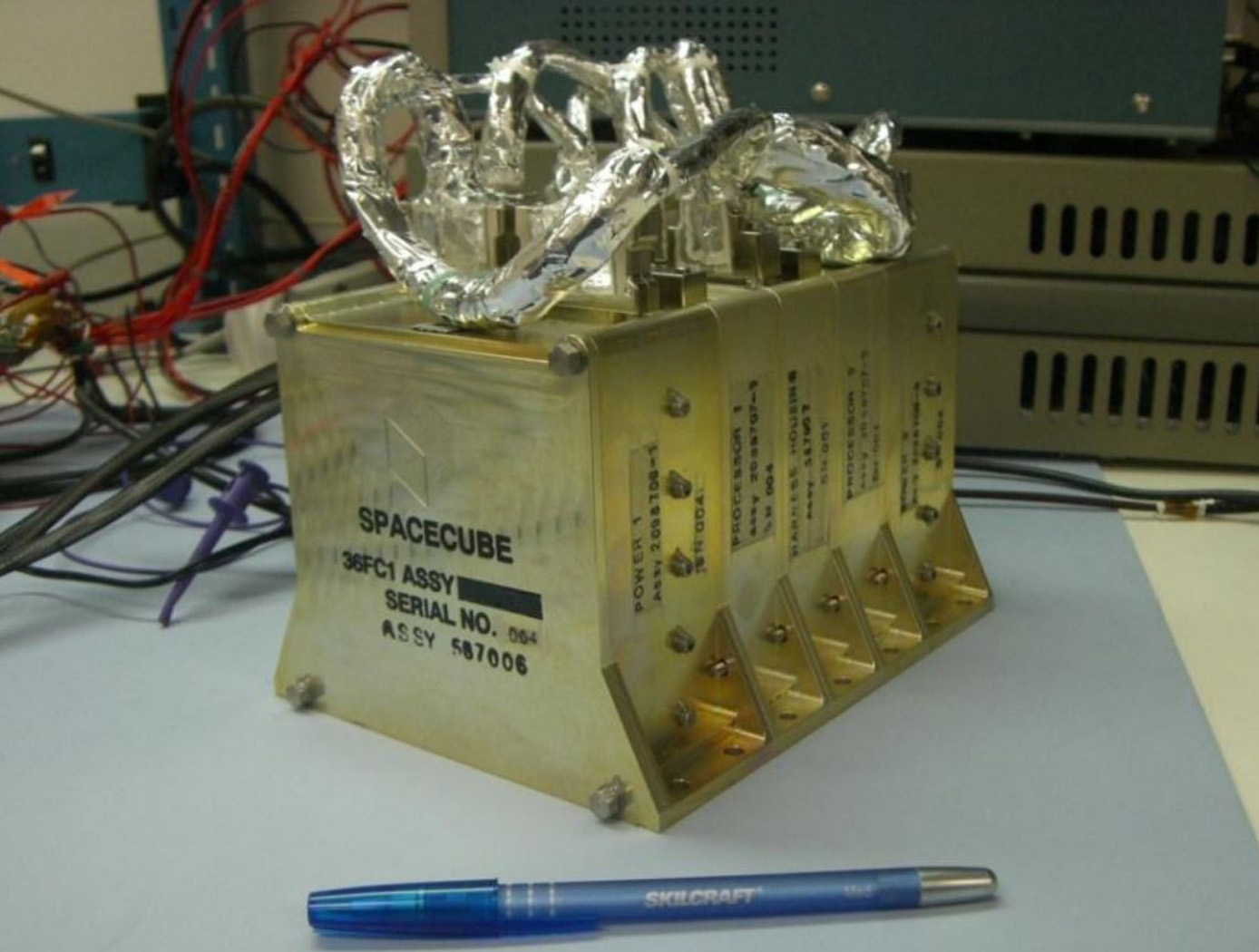
SpaceCube
Next generation instruments are capable of producing data at rates of 108 to 1011 bits per second, and both their instrument designs and mission operations concepts are severely constrained by data rate/volume. SpaceCube is an enabling technology for these next generation missions.
SpaceCube has demonstrated enabling capabilities in Earth Science, Planetary, Satellite Servicing, Astrophysics and Heliophysics prototype applications such as on-board product generation, intelligent data volume reduction, autonomous docking/landing, direct broadcast products, and data driven processing with the ability to autonomously detect and react to events. SpaceCube systems are currently being developed and proposed for platforms from small CubeSats to larger scale experiments on the ISS and standalone free-flyer missions, and are an ideal fit for cost constrained next generation applications due to the tremendous flexibility (both functional and interface compatibility) provided by the SpaceCube system.
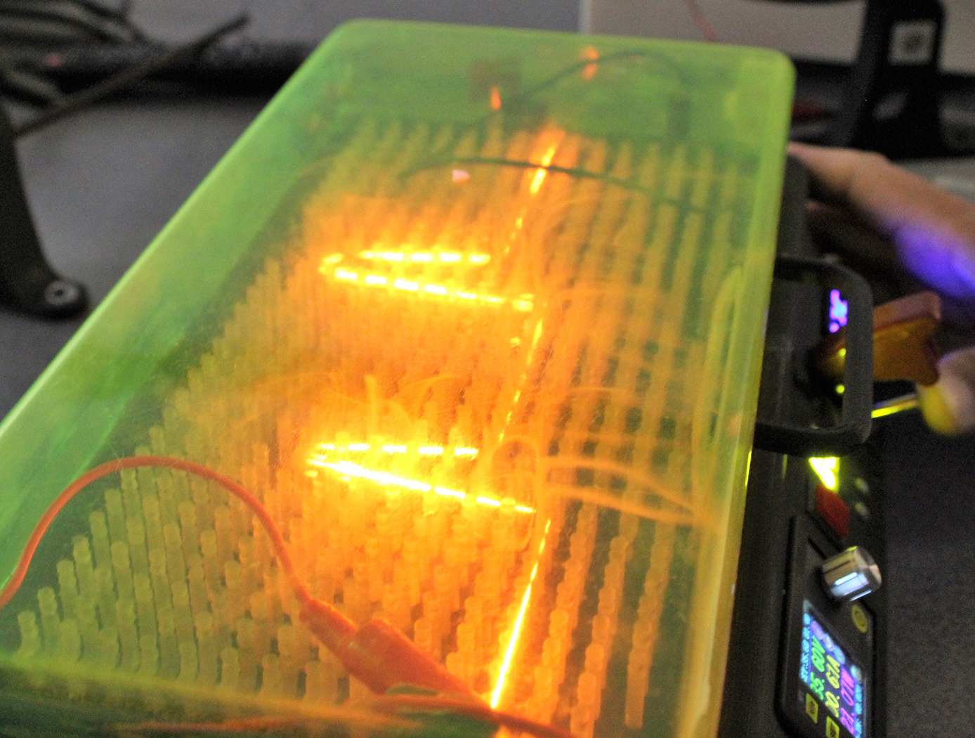
Shape Memory Alloy Art (SMArt)
A prototype device has been developed at Glenn for creating shapes from SMA wire. The apparatus uses material feedstock in spools made of alloys that exhibit the shape memory effect (temperature-induced activation), super elasticity (stress-induced activation), and to some extent, magnetism (magnetically-induced activation). The feedstock (e.g., wire spool) is routed and positioned around a series of modular pins to create a shape outline. Once the desired shape is formed, the wire ends are clipped from the feedstock and secured into a locking mechanism, then connected to a heating circuit (e.g., joule heating, hot plate, heat gun). The programmable prescribed circuit parameters, including current or temperature and training time, are set and confirmed using the apparatus control dials and indicators to ensure safe and accurate operation of the device. Before enabling the circuit, a plastic shield is placed over the modular array to protect the operator. The final product will be a desired shape that can be deformed and recovered numerous times through heat activation.

Serial Arrayed Waveguide Grating
Serial Arrayed Waveguide Grating enables higher resolution wavelength separation. Traditional AWGs split the optical signal into multiple parallel paths each with a different path length. This new approach creates the different path lengths by splitting the signal into essentially one long path in which the different channels are periodically split off the main path in the desired fraction. This has the net result of requiring much less space on-chip for comparable optical path differences.
In traditional AWG, there are multiple parallel optical paths, each with a different engineered path-length. For high resolution, you want many different parallel paths and large differences in path length between the paths. To design this on a photonics chip requires significant area. The serial AWG creates a single path, equivalent to the longest path in the parallel AWG and split off fractions of the optical signal at various points along the way to create the equivalent path lengths. Serial Arrayed Waveguide Grating re-uses the same path instead of needing independent parallel paths.
Robust High Temperature SiC Op Amps Practical Fabrication
The technology is part of a new generation of NASA Glenn SiC integrated circuits with unprecedented durability in the field of high-temperature electronics. For robust operational amplifiers based on SiC Junction Field Effect Transistors (JFETs), this novel compensation method mitigates issues with threshold voltage variations that are an effect of die location on the wafer. Modern high-temperature op amps on the market fall short due to temperature limits (only 225C for silicon-based devices). Previously, researchers noted that multiple op amps on a single SiC wafer had different amplification properties due to different threshold voltages that varied spatially as much as 18% depending on the circuit's distance from the SiC wafer center. While 18% is okay for some applications, other important system applications demand better precision. By applying this technology to the amplifier circuit design process, the op amp will provide the same signal gain no matter its position on the wafer. The compensation approach enables practical signal conditioning that works from 25C up to 500C.

Smooth-Walled Feed Horn
The technology is a monotonically-profiled, smooth-walled scalar feed horn optimized between 33 and 45 GHz. The phase center for this horn is near the aperture and is stable in frequency. The feed horns monotonic profile is compatible with machining by progressive plunge milling in which successively more accurate tools are used to realize the feed profile. This technique has been used for individual feeds and is potentially useful for fabricating large arrays of feed horns, such as multimode Winston concentrators, direct-machined smooth-walled conical feed horns, and for dual-mode feed horns.
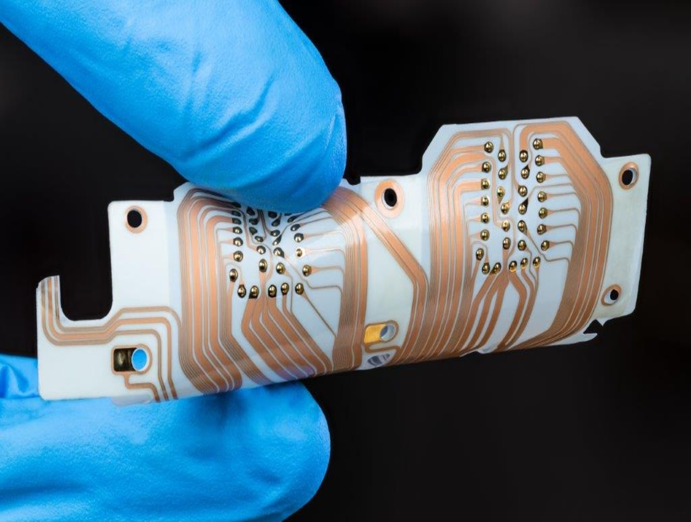
Printable IoT sensor development platform
Advances in additive manufacturing have enabled development of printable electronic sensor elements that can be deposited onto flexible substrates. To benchmark performance of printed sensors against the state of the art, NASA developed a low power flexible sensor platform. The platform integrates the following key components and features:
-Flexible substrate: DuPont Kapton allows bending around cylindrical surfaces as small as in diameter.
-Embedded microcontroller: Cypress CY8C4248 LQI-BL583 Arm Cortex M0 processor with BLE wireless controller, max frequency 48 MHz. Supports low power modes of operation, capacitive sensing support, and a single-channel 12-bit AD converter.
-Commercial sensor suite: Bosch BNO080 inertial sensor; Bosch BME280 humidity, pressure, and temperature sensor; AMS CCS811 air quality sensor (VOCs and CO2).
-Prototyping area for custom-printed sensors: 1) thermistor, uses carbon-based PTC resistor paste DuPont2792; 2) capacitive humidity sensor using a NASA-developed dielectric ink.
NASA researchers have used the platform to study performance of the printed capacitive humidity sensor. The 2x4 mm co-doped barium titanate sensing element is highly sensitive to water vapor and performs as an unobtrusive breathing monitor, sensitive to breath at distances of up to 20 cm. Average change of sensor capacitance at a distance of 7.5 cm was observed to be 6.23.5 pF.

Double Sided Si(Ge)/Sapphire/III-Nitride Hybrid Structures
III-nitride devices are commonly made on sapphire substrates today for various commercial electronic and optoelectronic applications. Thus, this innovation relates directly to the combination of devices on opposite sides of the sapphire substrate. One possible device combination is to have LEDs one side and solar cells on the other, such as for displays.

High Mobility Transport Layer Structures for Rhombohedral Si/Ge/SiGe Devices
Performance of solar cells and other electronic devices such as transistors can be improved greatly if carrier mobility is increased. Si and Ge have Type-II bandgap alignment in cubically strained and relaxed layers. Quantum well and super lattice with Si, Ge, and SiGe have been good noble structures to build high electron mobility layer and high hole mobility layers. However, the atomic lattice constant of Ge is bigger than that of Si and direct epitaxial growth generates large density of misfit dislocations which decrease carrier mobility and shorten device life time. So it required special buffer layers such as super lattice or gradient indexed layers to grow Ge on Si wafers or Si on Ge wafers. The growth of these buffer layers takes extra effort and time such as post-annealing process to remove dislocations by dislocation gliding inside buffer layer.
This invention is a fabrication method for high mobility layer structures of rhombohedrally aligned SiGe on a trigonal substrate. The invention utilizes C-plane (0001) Sapphire which has a triangle plane, and a Si (Ge) (C) (111) crystal or an alloy of group TV semiconductor (111) crystal grown on the Sapphire.

Concept Development for Advanced Spaceborne Synthetic Aperture Radar
The current innovation utilizes heritage flight proven L-band Digital Beamforming Synthetic Aperture Radar (DBSAR) in conjunction with a new P-Band Digital beamforming Polarimetric and Interferometric EcoSAR (ESTO IIP) architecture. The system employs digital beamforming (DBF) and reconfigurable hardware to provide advanced radar capabilities not possible with conventional radar instruments. The SAR is operated without the use of a slewing antenna allowing the single radar system to provide polarimetric imaging, interferometry, and altimetry or scatterometry data types. The SAR is also capable of Sweep-SAR, simultaneous SAR/GNSS-R , and simultaneous active/passive techniques.
This system has an increased coverage area and can rapidly image large areas of the surface using the simultaneous left/right imaging. The resulting images maintain their full resolution and allows for faster full coverage mapping
View more patents

