Search
electrical and electronics
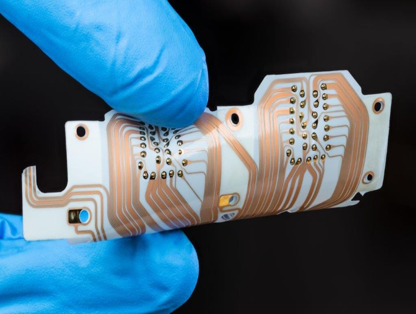
Printable IoT sensor development platform
Advances in additive manufacturing have enabled development of printable electronic sensor elements that can be deposited onto flexible substrates. To benchmark performance of printed sensors against the state of the art, NASA developed a low power flexible sensor platform. The platform integrates the following key components and features:
-Flexible substrate: DuPont Kapton allows bending around cylindrical surfaces as small as in diameter.
-Embedded microcontroller: Cypress CY8C4248 LQI-BL583 Arm Cortex M0 processor with BLE wireless controller, max frequency 48 MHz. Supports low power modes of operation, capacitive sensing support, and a single-channel 12-bit AD converter.
-Commercial sensor suite: Bosch BNO080 inertial sensor; Bosch BME280 humidity, pressure, and temperature sensor; AMS CCS811 air quality sensor (VOCs and CO2).
-Prototyping area for custom-printed sensors: 1) thermistor, uses carbon-based PTC resistor paste DuPont2792; 2) capacitive humidity sensor using a NASA-developed dielectric ink.
NASA researchers have used the platform to study performance of the printed capacitive humidity sensor. The 2x4 mm co-doped barium titanate sensing element is highly sensitive to water vapor and performs as an unobtrusive breathing monitor, sensitive to breath at distances of up to 20 cm. Average change of sensor capacitance at a distance of 7.5 cm was observed to be 6.23.5 pF.
Sensors

Capacitive Impedance Water Ice Sensor (CIWIS)
The CIWIS is configured to detect ice, water, and other material accretion on an aircraft's surface using a capacitive sensor comprised of metal traces on a printed circuit board (PCB) with a dielectric surface covering. The traces are on the bottom side of the PCB for protection from the elements experienced on the top side. It drives the sensor with a sinusoidal signal and monitors the sensed sinusoidal signal from the sensor. By electronically measuring the RMS voltage of both the drive and sensed signal as well as the phase shift introduced by the sensor, the CIWIS can determine the impedance of the sensor and any material deposition. When a material is present on the surface, this introduces another capacitor in parallel with the air and PCB, with that material being another dielectric.
Water and ice exhibit frequency-dependent permittivity that introduces a phase shift unlike that of a typical capacitor. CIWIS leverages these differences, distinguishing materials by the unique RMS levels and phase shifts they produce in the sensor. For ice, this effect occurs at approximately 10 kHz.
While NASA originally developed the CIWIS to detect ice on aircraft, it may also be useful to sense the presence of water and other contaminants in pharmaceutical production; condensation in heating, ventilation, and air conditioning (HVAC) systems; and ice accumulation on cryogenic equipment. This technology is available for patent licensing, and is rated at a Technology Readiness Level or TRL of 5 , meaning it has been developed and validated in an industrially relevant environment and is ready for a prototype demonstration.
Sensors

Thin Film Sensor for Ultra High-Temp Measurement
The thin film sensor’s principal advantage lies in its potential to take high frequency temperature measurements from the surface of a reentering spacecraft while simultaneously withstanding the high temperature and oxidizing environment encountered. This data provides engineers with operational phase measurements used to refine the spacecraft’s operational envelope and track flight hardware behavior in addition to providing high frequency temperature measurements that can inform the physics of a boundary layer.
Mismatches in coefficients of thermal expansion (CTE) are expected in TPS-based sensor applications because the metallic materials used for temperature sensing have thermal expansion rates that differ from the rates of the substrate and coating materials in the TPS. At high temperatures during reentry, this mismatch in CTE can create a significant strain differential between the metallic sensor, sensor leads, and the materials to which the sensor and leads are bonded.
High frequency response temperature measurements on the surface of entry spacecraft are not currently possible above ~700 F with existing measurement capabilities. This shortcoming is primarily due to the need for robust sensor behavior at temperatures of several thousand degrees F. The sensor design of this technology preserves the integrity of sensor components while enhancing its high temperature functionality.
The thin film temperature sensor has a technology readiness level (TRL) 5 (Component and/or breadboard validation in relevant environment) and is now available for patent licensing. Please note that NASA does not manufacture products itself for commercial sale.
Sensors

Hybrid carbon nanotube-gold nanoparticle composite for Nitric Oxide (NO) detection
A hybrid thin film is fabricated by a simple drop-casting method. Functionalized single-walled carbon nanotubes (SWCNTs) and gold nanoparticles (AuNPs) with a diameter of ≈15 nm are drop-casted onto a printed circuit board (PCB) substrate equipped with interdigitated electrodes. The addition of AuNPs to the carbon nanotube networked films enhance sensitivity and lower the detection limit to low parts-per-billion (ppb) concentrations. The gold particle to carbon nanotube ratio is optimized to find the optimum gold nanoparticle loading.
The composite films were tested in both air and nitrogen environments across a wide relative humidity range (0-97%), which is suitable for dissolved Nitric Oxide (NO) detection in sea water for oceanographic study and for human breath analysis in medical diagnosis. The sensors exhibited high selectivity, particularly to NO, outperforming other tested gases. Notably, the sensor reliably detected NO at 10 ppb levels with response times within 10 seconds and recovery time around 1 minute, showcasing excellent reproducibility across sensors and operational efficiency within diverse humidity conditions.
sensors
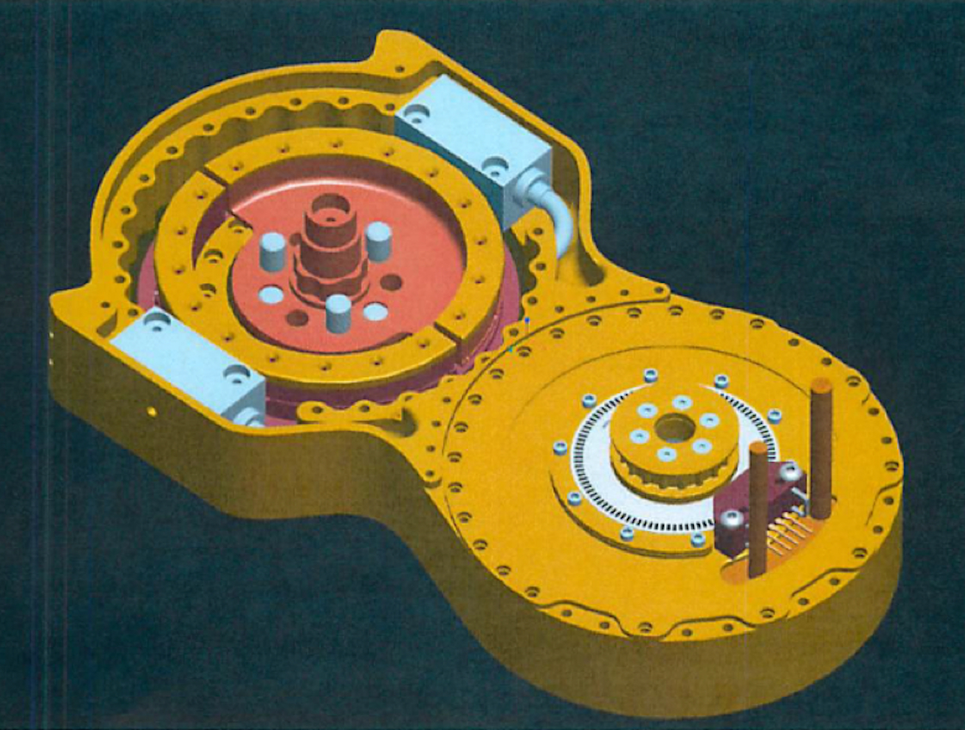
Split-Ring Torque Sensor
The SRTS enables measurement of position, velocity, and torque of a rotating system (e.g., actuator, motor, crankshaft, rotor, etc.) using two optical sensors and a single, custom-designed split-ring rather than the standard dual-ringed systems commonly used for similar applications. The split-ring is comprised of two structural arcs positioned in a concentric, coplanar relationship, wherein each arc is attached to a component capable of rotation (e.g., a lower leg and upper leg, where the SRTS acts as a knee). The two arcs contain indications or codes on their outer surfaces that are read by the optical sensors to determine the relative deflection of the structural arcs as they rotate.
The SRTS configuration discussed above is limited to 180-degree applications. The addition of a third structural arc and a third optical reader, however, would enable 360-degree functionality.
Tests have shown the SRTS has a high degree of tolerance to temperature differences and provides higher resolution measurements than competing technologies.
electrical and electronics
Robust High Temperature SiC Op Amps Practical Fabrication
The technology is part of a new generation of NASA Glenn SiC integrated circuits with unprecedented durability in the field of high-temperature electronics. For robust operational amplifiers based on SiC Junction Field Effect Transistors (JFETs), this novel compensation method mitigates issues with threshold voltage variations that are an effect of die location on the wafer. Modern high-temperature op amps on the market fall short due to temperature limits (only 225C for silicon-based devices). Previously, researchers noted that multiple op amps on a single SiC wafer had different amplification properties due to different threshold voltages that varied spatially as much as 18% depending on the circuit's distance from the SiC wafer center. While 18% is okay for some applications, other important system applications demand better precision. By applying this technology to the amplifier circuit design process, the op amp will provide the same signal gain no matter its position on the wafer. The compensation approach enables practical signal conditioning that works from 25C up to 500C.
Sensors

Dust Accumulation Sensor Provides In Situ Monitoring
Previous techniques for measuring dust accumulation, mostly de-pendent on solar cell output, were limited by their inability to distin-guish dust effects from other factors like incident radiation and radiation damage. These techniques were less effective in environ-ments with inconsistent solar flux and future missions, such as the Lunar South Pole, and lacked versatility in adapting to diverse envi-ronmental conditions. The PADS device embraces success over these challenges, and reflects enhanced features over prior iterations to also allow for space environments.
Key design features begin with the customizable mechanical design of the PADS device for use in space environments, heaters with imbedded precision temperature sensors, a selected optical coating for the device coupons that are calibrated on high-fidelity thermal modeling and validated with ground-based testing to simulate the space environment of interest (including dusting with simulants representative of the planetary-body soil/regolith), and a control circuit for precision control/matching of the thermal inputs to the sensor via the heaters. Retainers with mount isolators are implemented to ensure the stacked layers within the device do not dislodge during high vibration or gravitational loads during launch.
For operation, the PADS device is installed at the point of interest (e.g., space vehicle surface, extraterrestrial equipment) to quantify dust accumulation. Power and data transfer are done through cabling to the space vehicle system or can be provided standalone. A control circuit/algorithm adjusts the power to the heaters to precisely match the temperature setpoints. Ground testing in the simulated space environment conditions of interest creates a calibration plot of effec-tive emittance versus dust density, and allows determination of the degradation in emittance as the dust increases on the surface.
Testing on the PADS device has been completed in a simulated lunar environment and data has been collected to enable sensor calibration for its use on the Moon. It is currently poised for integration into a lander for flight testing.
Although the PADS device is intended for use in a burgeoning space industry and requisite environments – but given that the PADS device is partially comprised of programmable sensors in conjunction with optically coated coupons that can be tailored for custom use - it or its constituent components could be modified for terrestrial applications such as surface dust monitoring on photovoltaic panels or potentially combustible dust on various industrial surfaces.
instrumentation
Portable Medical Diagnosis Instrument
The technology utilizes four cutting-edge sensor technologies to enable minimally- or non-invasive analysis of various biological samples, including saliva, breath, and blood. The combination of technologies and sample pathways have unique advantages that collectively provides a powerful analytical capability. The four key technology components include the following: (1) the carbon nanotube (CNT) array designed for the detection of volatile molecules in exhaled breath; (2) a breath condenser surface to isolate nonvolatile breath compounds in exhaled breath; (3) the miniaturized differential mobility spectrometer (DMS) -like device for the detection of volatile and non-volatile molecules in condensed breath and saliva; and (4) the miniaturized circular disk (CD)-based centrifugal microfluidics device that can detect analytes in any liquid sample as well as perform blood cell counts. As an integrated system, the device has two ports for sample entry a mouthpiece for sampling of breath and a port for CD insertion. The breath analysis pathway consists of a CNT array followed by a condenser surface separating liquid and gas phase breath. The exhaled breath condensate is then analyzed via a DMS-like device and the separated gas breath can be analyzed by both CNT sensor array again and by DMS detectors.
Aerospace
eVTOL UAS with Lunar Lander Trajectory
This NASA-developed eVTOL UAS is a purpose-built, electric, reusable aircraft with rotor/propeller thrust only, designed to fly trajectories with high similarity to those flown by lunar landers. The vehicle has the unique capability to transition into wing borne flight to simulate the cross-range, horizontal approaches of lunar landers. During transition to wing borne flight, the initial transition favors a traditional airplane configuration with the propellers in the front and smaller surfaces in the rear, allowing the vehicle to reach high speeds. However, after achieving wing borne flight, the vehicle can transition to wing borne flight in the opposite (canard) direction. During this mode of operation, the vehicle is controllable, and the propellers can be powered or unpowered.
This NASA invention also has the capability to decelerate rapidly during the descent phase (also to simulate lunar lander trajectories). Such rapid deceleration will be required to reduce vehicle velocity in order to turn propellers back on without stalling the blades or catching the propeller vortex. The UAS also has the option of using variable pitch blades which can contribute to the overall controllability of the aircraft and reduce the likelihood of stalling the blades during the deceleration phase.
In addition to testing EDL sensors and precision landing payloads, NASA’s innovative eVTOL UAS could be used in applications where fast, precise, and stealthy delivery of payloads to specific ground locations is required, including military applications. This concept of operations could entail deploying the UAS from a larger aircraft.
sensors

Solid State Carbon Dioxide (CO2) Sensor
The technology is a solid state, Carbon Dioxide (CO2) sensor configured for sensitive detection of CO2 having a concentration within the range of about 100 Parts per Million (ppm) and 10,000 ppm in both dry conditions and high humidity conditions (e.g., > 80% relative humidity). The solid state CO2 sensor achieves detection of high concentrations of CO2 without saturation and in both dynamic flow mode and static diffusion mode conditions. The composite sensing material comprises Oxidized Multi-Walled Carbon Nanotubes (O-MWCNT) and a metal oxide, for example O-MWCNT and iron oxide (Fe2O3) nanoparticles. The composite sensing material has an inherent resistance and corresponding conductivity that is chemically modulated as the level of CO2 increases. The CO2 gas molecules absorbed into the carbon nanotube composites cause charge-transfer and changes in the conductive pathway such that the conductivity of the composite sensing material is changed. This change in conductivity provides a sensor response for the CO2 detection. The solid state CO2 sensor is well suited for automated manufacturing using robotics and software controlled operations. The solid state CO2 sensor does not utilize consumable components or materials and does not require calibration as often as conventional CO2 sensors. Since the technology can be easily integrated into existing programmable electronic systems or hardware systems, the calibration of the CO2 sensor can be automated.

