Search
sensors
Room temperature oxygen sensors
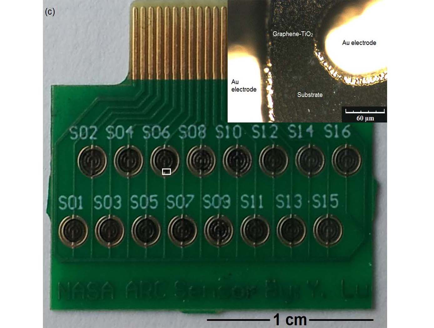
NASA Ames has developed very small-sized oxygen sensors made of a graphene and titanium dioxide (TiO<sub>2</sub>) hybrid material. With ultraviolet (UV) illumination, these sensors are capable of detecting oxygen (O<sub>2</sub>) gas at room temperature and at ambient pressure. The sensors are able to detect oxygen at concentrations ranging from about 0.2% to about 10% by volume under 365nm UV light, and at concentrations ranging from 0.4% to 20% by volume under short wave 254nm UV light. These sensors have fast response and recovery times and can also be used to detect ozone.
This unique room temperature O<sub>2</sub> sensor provides significant advantages in O<sub>2</sub> sensing applications, especially those applications where high operating temperature requirements cannot be met, or would result in inefficient manufacturing processes. Since graphene is not intrinsically responsive to O<sub>2</sub>, and TiO<sub>2</sub> is not responsive to oxygen at room temperature, the materials are first synthesized as a hybrid material. The synthesized graphene- TiO<sub>2</sub> hybrid material is then ultrasonicated and then drop-casted onto a series of Interdigitated Electrodes (IDE) to form the sensors.
Ultrasonication ensures effective charge transfer at the graphene- TiO<sub>2</sub> interphase. The graphene and the titanium dioxide may be present in the composite material in different ratios to ensure optimal oxygen detection. It is the combination of graphene with TiO2 that yields a semiconducting material capable of O<sub>2</sub> sensing at room-temperature operation.
Manufacturing

Fabrication of Binary Phase Photon Sieves
This NASA invention is an innovative process for fabricating high-area binary phase photon sieves with improved optical efficiency for EUV imaging applications. Binary phase photon sieves have been demonstrated for a variety of optical and x-ray applications. Photon sieves must be wide, super-thin, and etched with precise holes to refract light. Each step in NASA's photon sieve fabrication process includes considerations to protect the resulting sieves, such as leaving a honeycomb of thicker material to support the membrane and prevent tearing. The process starts by using a silicon-on-insulator wafer, includes pattern and etch-sieve pattern, and ends with a released photon sieve. The inventors have produced an 8 cm-diameter silicon sieve that is 100 nm thick including hole sizes of 2 µm in diameter with 2 µm spacing. Additionally, a similar structure has been demonstrated in niobium, with 8 cm in diameter with the same silicon hexagonal support frame.
This novel process enables the fabrication of photon sieves for EUV imaging applications. While the process was initially developed to fabricate photon sieves for solar science and astronomy, it could also be used to generate metamaterial/frequency selective surface structures from the UV to THz frequency ranges. This NASA invention is a Technology Readiness Level (TRL) 4 (prototype validation in a laboratory environment) technology and is available for patent licensing.
Manufacturing

Novel Process to Create Structured Membrane Films for Micromachining Applications
The technology is an innovative process for creating metal-patterned, structured membranes for micromachining applications. The method uses potassium hydroxide to remove silicon, in combination with XHRiC. Hafnium metal is first patterned onto a silicon nitride wafer, which serves as the starting substrate. XHRiC is then applied to the wafer, followed by patterning with photoresist and etching using O2 plasma to define cut slots in the membrane. The photoresist is then removed.
Next, the wafer is bonded to a Pyrex carrier wafer with wax, and the backside of the silicon nitride is patterned and reactive-ion etched. The wafer is then placed in hot potassium hydroxide for 16 hours to remove the silicon layer, creating a silicon nitride membrane. The wafer is subsequently placed in acetone to dissolve the wax. The wafer is resecured to the Pyrex carrier wafer, and the topside of the silicon nitride membrane is subjected to reactive-ion etching. Finally, the XHRiC layer is removed using O2 plasma, and the Pyrex handle wafer is released, resulting in a metal-patterned silicon nitride membrane with cut slots.
This novel process supports the creation of structured membranes with a wide range of applications in MEMS fabrication. The use of XHRiC as a patterned hard mask and/or etch protection material enables its application in various MEMS devices. The process can be used to fabricate cut membranes, micro/nano structures, and ultra-thin films for device applications, making it an excellent candidate for MEMS foundry companies and accelerometer manufacturers. It has reached a Technology Readiness Level (TRL) 5 (component validation in a relevant environment) and is now available for patent licensing.
Robotics Automation and Control
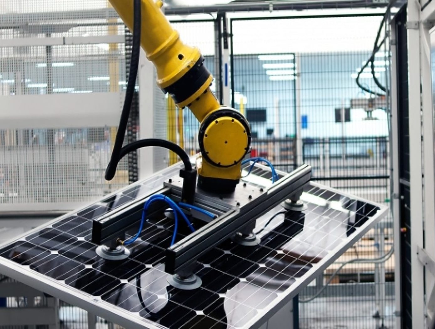
Robotic Assembly of Photovoltaic Arrays
NASA researchers have developed the PAPA technology to increase the efficiency of the thin-film solar array assembly process, significantly decreasing assembly time and labor costs associated with manufacturing large scale solar arrays. Traditional solar cell assembly is a labor intensive, multi-step, time-consuming process. This manual assembly will not be possible in a space environment. To enable solar array assembly in space, PAPA leverages robotic automation to distill the traditional assembly method into four fully automated steps: applying adhesive to block substrate, placing the solar cells using a vacuum tool attached to a universal robotic arm, printing the interconnects and buses to connect the cells, and applying a protective cover.
The PAPA technology is compatible with a variety of thin-film solar cells, including 3D printed cells (essential for future in-space manufacturing of arrays) and terrestrial manufacturing methods. As solar cell technologies mature, PAPA will be able to incorporate advancements into the paneling process. NASA researchers have begun to employ PAPA solar array fabrication and estimate savings of $300-$400/watt. For extraterrestrial assembly of solar panels the size of a football field or larger, PAPA could result in savings of approximately $500 million; a substantial cost savings driven by standardization and efficiency in the solar array assembly process. By demonstrating increases in assembly efficiency, time and cost savings, and passing multiple environmental exposure tests, the PAPA lab protype has completed the final phases of technology development and is ready for scale-up and commercialization.
Manufacturing

Rapid Aerogel Prototyping Using 3D Printing
To overcome the challenges of conventional molding, researchers at NASA Glenn have developed a rapid prototyping approach for three-dimensional printing of polymer aerogels using deposition into a viscous, sacrificial support medium. The sacrificial support stabilizes the aerogel deposition, allowing precise layer-by-layer construction of self-supporting aerogel networks that would otherwise be unprintable in air. Following printing and gelation of the polymer network, the printed structure is gently removed from the sacrificial medium, yielding a freestanding aerogel precursor with high shape fidelity.
This method decouples printability from intrinsic material viscosity and enables rapid iteration of aerogel geometries, offering a scalable pathway for additive manufacturing of ultra-lightweight, architected polymer aerogels with tailored geometries, while retaining microstructural, mechanical, and thermal properties.
The method involves:
1. Forming a solution comprised of a polymer precursor, cross-linker, solvent, and catalyst to create a dilute polymer solution.
2. 3D printing the polymer precursor directly into the sacrificial support medium.
3. Following printing and network formation, the structure is removed from the sacrificial medium through a low-stress extraction process, yielding a freestanding polymer aerogel precursor that retains the as-printed geometry with high fidelity.
The sacrificial medium functions as a temporary, conformal support matrix that stabilizes each deposited droplet or filament in situ, enabling freeform construction of aerogel. This strategy enables the fabrication of highly porous, interconnected networks with controlled feature resolution across multiple length scales, while maintaining the intrinsic low density and high surface area required for aerogel performance.

