Search
propulsion
Sublimable Propellant Source for Iodine-fed Ion Propulsion System
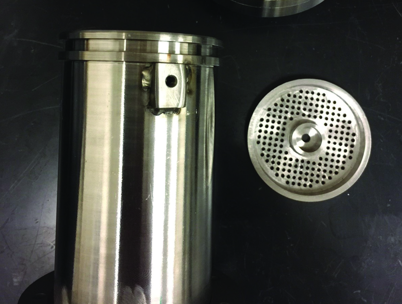
NASAs iodine vapor feed system is based on a mechanism that holds and maintains the solid iodine is contact with a heated surface, in this case the walls of the propellant tank. The mechanism provides a robust and reliable steady-state delivery of sublimated iodine vapor to the ion propulsion system by ensuring good thermal contact between the solid iodine and the tank walls.
To date, the technology development effort includes extensive thermal, mechanical and flow modelling together with testing of components and subsystems required to feed iodine propellant to a 200-W Hall thruster. The feed system has been designed to use materials that are resistant to the highly-reactive nature of iodine propellant. Dynamic modeling indicates that the feed system tubing can be built is such a way as to reduce vibrationally-induced stresses that occur during launch. Thermal modeling has been performed to demonstrate that the feed system heater power levels are sufficient to heat the tank and propellant lines to operating temperatures, and sublime the iodine in the storage tank to supply propellant for reliable and long-term operation.
Materials and Coatings

Advanced AlF3-Passivated Aluminum Mirrors
NASA’s innovative passivation process consists of exposing in-situ Physical Vapor Deposited oxide-free AI samples in a high or ultra-high vacuum chamber at ambient temperature to a low-pressure reactive gas of xenon difluoride (XeF2) immediately after depositing the AI layer. In this chemisorption process, the XeF2 is adsorbed on the surface of the AI layer, and due to the affinity of Al to fluorine molecules, the weakly-bound Xe dissociates and is pumped out of the chamber. A thin AlF3 overcoat layer is produced as a result.
Other embodiments of the invention include the use of alternative processing gasses for the passivation treatment, or the utilization of a plasma source to increase the ion/atom ratio of the incident fluorine species resulting after XeF2 dissociation. Similarly, different mirror substrates materials with suitable surface characteristics in the FUV could be employed.
In addition to the improved FUV reflectance, environmental stability, and maintained efficiency at higher wavelengths of the resulting Al mirrors, this NASA process has several unique features. Firstly, the entire process is carried out at ambient temperature, eliminating the need for high-temperature fluoride deposition. Secondly, the process is highly scalable, limited only by the size of the coating chamber where the passivation of XeF2 is carried out. Finally, the process can be manipulated to conform to any geometry, enabling its use for curved optics.
While NASA originally developed the passivation of oxide-free aluminum coatings to realize reflectivity enhancement in the Far-Ultraviolet for the Large UV/Optical/IR Surveyor (LUVOIR), it may also be useful to companies that manufacture ground-based or space-based optical systems with sensitivity to the FUV spectrum. Examples include optics for space telescopes with reflective elements, vacuum-ultraviolet (VUV) plasma analysis tools, photolithography instrumentation, and wafer inspection tools.
Materials and Coatings

Self-Cleaning Coatings for Space or Earth
The new transparent EDS technology is lighter, easier to manufacture, and operates at a lower voltage than current transparent EDS technologies. The coating combines an optimized electrode pattern with a vapor deposited protective coating of SiO2 on top of the electrodes, which replaces either polymer layers or manually adhered cover glass (see figure on the right). The new technology has been shown to achieve similar performances (i.e., over 90% dust clearing efficiency) to previous technologies while being operated at half the voltage.
The key improvement of the new EDS coating comes from an innovative method to successfully deposit a protective layer of SiO2 that is much thinner than typical cover glass. Using vapor deposition enables the new EDS to scale more successfully than other technologies that may require more manual manufacturing methods. The EDS here has been proven to reduce dust buildup well under vacuum and may be adapted for terrestrial uses where cleaning is done manually. The coatings could provide a significant improvement for dust removal of solar cells in regions (e.g., deserts) where dust buildup is inevitable, but water access is limited. The EDS may also be applicable for any transparent surface that must remain transparent in a harsh or dirty environment.
The related patent is now available to license. Please note that NASA does not manufacturer products itself for commercial sale.
Materials and Coatings
Epitaxy of SiGe and Other Compound Semiconductors
Several of the patented methods included in this suite of technologies enable super-hetero-epitaxy of rhombohedral/cubic compound semiconductors on specially oriented trigonal (e.g. sapphire) or hexagonal (e.g. quartz) crystal wafer substrates. This includes alignment of the growth crystal lattice with the underlying substrate lattice to minimize misfit strain-induced dislocation defects in the growing crystal. Thus thicker, defect-free crystal layers can be made. Rhombohedral/Cubic crystal twin defects which is 60 degree rotated on [111] orientation in a rhombohedral/cubic SiGe layer structure can be reduced to well less than 1% by volume, essentially providing a defect-free semiconductor material. Alternately, engineered lattice structures with a high degree of twinning can provide SiGe with improved thermoelectric properties due to the phonon scattering that inhibits thermal conduction without compromising electrical conductivity. Additional patented technologies in this suite provide for physical vapor deposition (PVD) growth methods utilizing molten sputtering targets and thermal control of heated substrates, including electron beam heating, in order to give the atoms in the sputtered vapor or on the substrate surface the energy needed for the desired crystal growth.
The remaining patented technologies enable x-ray diffraction methods for detecting and mapping crystal twin defects across the entire as-grown semiconductor layer. These defects are critical to the performance of any semiconductor device manufactured from such compound semiconductor materials.
Mechanical and Fluid Systems

Passive Fuel Cell Surface Power System (PaCeSS)
NASA’s envisioned Lunar and Martian surface operations will require constant and reliable power systems. Traditional power architectures, including solar cells and batteries, cannot be solely relied upon due to the lengthy lunar nights and challenging thermal environments. How-ever, fuel cells, including primary fuel cells and regenerative fuel cells, represent a promising means for energy generation and storage on planetary and lunar surfaces.
PaCeSS could further improve mission flexibility by significantly enhanc-ing reliability and longevity with fully passive fuel cell power generation capability. Test systems have been built to validate the performance characteristics of various PaCeSS technology elements, and many of the component materials have already been characterized. Some of these novel technology elements already demonstrated include a two-phase thermosyphon operation in fuel cell conditions, a passive shape memory actuator operation using two-phase water, and a shape memory alloy radiator turndown.
Although the current design of the shape memory alloy actuated rad-iator system is dependent on partial gravity and space-like environments where heat rejection is performed primarily via radiation, there may be ways of using the same basic system for controlling fuel cell temper-ature via convective heat rejection for terrestrial applications. Addition-ally, other elements of this concept could be commercialized terrestri-ally, including the thermosyphon heat transport mechanism, a multi-purpose vapor chamber, and a thermal management system that uses water by-product as the thermal management medium.
The Passive Fuel Cell Surface Power System is at a technology readiness level (TRL) 3 (analytical and experimental critical function and/or characteristic proof of concept) and is now available for patent licensing. Please note that NASA does not manufacture products itself for commercial sale.

