SiC-Based Microstructures for Sensors
sensors
SiC-Based Microstructures for Sensors (LEW-TOPS-128)
Ultra-thin SiC microstructures enable batch fabrication of MEMS, NEMS, pressure sensors, and biosensors
Overview
Innovators at NASA's Glenn Research Center have developed ultra-thin silicon carbide (SiC) microstructures that enable highly sensitive pressure sensors that are bio-compatible. The novel method of fabricating these microstructures, Dopant Selective Reactive Ion Etching (DSRIE), allows for structures as thin as 2 microns to be achieved, while allowing multifunctional sensors to be fabricated on a single SiC wafer. For the first time, it is possible to batch-fabricate ultra-thin SiC diaphragms that can sense very low pressures, enabling pressure sensors that can measure sub-psi pressures. This faster process makes it easier and less costly to produce complex, advanced semiconductors that are fully functional at temperatures greater than 600°C. This technique enables a new generation of SiC-based microelectromechanical systems (MEMS) and nanoelectromechanical systems (NEMS) such as accelerometers, pressure sensors, and biosensors.
The Technology
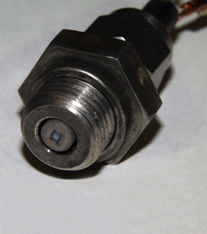
Glenn's invention is game-changing in its ability to produce ultra-thin SiC-based microstructures and diaphragms that are essential for high-sensitivity pressure sensors that not only monitor engines but can also act as biosensors (monitoring bone density or brain pressure). DSRIE offers selective etching that reliably isolates conductive microstructures from the bulk material and has precision-etch control that minimizes yield loss due to manufacturing defects. Therefore, the thickness of structures, such as diaphragms, can be ultra-thin and selectively realized during dopant reactive ion etching. The ultra-thin diaphragm is a key enabler for Glenn's novel pressure sensor that can measure at low pressures in the sub-psi range.
Until now, batch fabrication of SiC sensors has been hindered by the fact that only one type of sensor per wafer could be produced at a time. Given the expense of fabrication, this limitation has greatly reduced the commercial viability of SiC sensors and electronics. Glenn's batch fabrication offers manufacturers the opportunity to simultaneously produce multiple multifunctional MEMS/NEMS products on a single SiC wafer. Such products include flow sensors, pressure sensors, biosensors, accelerometers, inertial sensors, angular rate sensors, and yaw rate sensors. By simplifying production, reducing capital equipment, and lowering production costs, Glenn's novel process makes the use of SiC-based MEMS/NEMS in sensors and electronics much more practical and attainable for countless industries.


Benefits
- Ultra-thin: Overcomes conventional reactive ion etching limitations that can accurately fabricate microstructures as thin as 2 microns
- Low-cost: Enables batch fabrication, reducing the complexity and thereby cost associated with conventional fabrication techniques
- High-yield: Offers precision etch control that minimizes yield loss due to defects
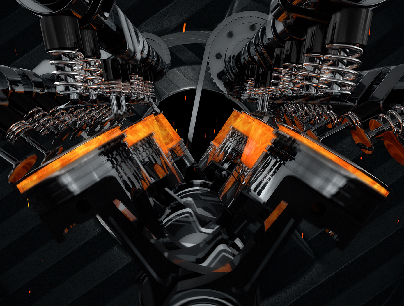
- Reliable: Enables SiC sensors to be placed within an engine combustion chamber, improving the fidelity and accuracy of data
- High-Sensitivity: Enables SiC-based MEMS/NEMS such as pressure sensors and biologically compatible probes and implants
Applications
- Automotive engines
- Highly sensitive pressure sensors
- Power generation
- Oil and gas exploration
- Battery membranes
- Aerospace
- Biosensors
- High-temperature sensors
- Electronics
Similar Results

Metallization for SiC Semiconductors
To avoid catastrophic failure, traditional electrical ohmic contacts must be placed at some distance from the optimal position (especially for sensors) in high-temperature environments. In addition, conventional metallization techniques incur significant production costs because they require multiple process steps of successive depositions, photolithography, and etchings to deposit the desired ohmic contact material. Glenn's novel production method both produces ohmic contacts that can withstand higher temperatures than ever before (up to 600°C), and permits universal and simultaneous ohmic contacts on n- and p-type surfaces. This makes fabrication much less time-consuming and expensive while also increasing yield. This innovative approach uses a single alloy conductor to form simultaneous ohmic contacts to n- and p-type 4H-SiC semiconductor. The single alloy conductor also forms an effective diffusion barrier against gold and oxygen at temperatures as high as 800°C. Glenn's extraordinary method enables a faster and less costly means of producing SiC-based sensors and other devices that provide quicker response times and more accurate readings for numerous applications, from jet engines to down-hole drilling, and from automotive engines to space exploration.

Packaging for SiC Sensors and Electronics
Prior approaches to bonding a SiC sensor and a SiC cover member relied on either electrostatic bonding or direct bonding using glass frits. The problem with the former is that its relatively weak bond strength may lead to debonding during thermal cycling, while the latter requires the creation of apertures that can allow sealant to leak. Glenn's innovation uses NASA's microelectromechanical system direct chip attach (MEMS-DCA) technology that can be bulk-manufactured to reduce sensor costs. The MEMS-DCA process allows a direct connection to be made between chip and pins, thereby eliminating wire bonding. Sensors and electronics are attached in a single-stage process to a multifunctional package, which, unlike previous systems, can be directly inserted into the housing. Additional thick pins within the electrical outlet allow the package to be connected to external circuitry. Furthermore, because the top and bottom substrates' thermomechanical properties are similar to that of the sensors, the problem of mismatch in the coefficient of thermal expansion is significantly reduced, minimizing thermal cycling and component fatigue. By protecting sensors and electronics in temperatures up to 600°C, approximately twice what has previously been achievable, Glenn's innovation enables SiC components to realize one of their most exciting possibilities - direct placement within high-temperature environments.

Advanced Hydrogen and Hydrocarbon Gas Sensors
In conjunction with academia and industry, NASA's Glenn Research Center has developed a range of microelectromechanical systems (MEMS)-based and Silicon Carbide (SiC)-based microsensor technologies that are well-suited for many applications. The suite of technologies includes hydrogen and hydrocarbon leak detection sensors; emissions sensor arrays; and high-temperature contact pads for wire bond connections.
Currently used to protect astronauts on the International Space Station, the hydrogen and leak detection sensors have many Earth-based applications as well. They can function as a single-sensor unit or as part of a complete smart sensor system that includes multiple sensors, signal conditioning, power, and telemetry. The system can comprise sensors for hydrogen, hydrocarbons, oxygen, temperature, and pressure. The emissions sensor array features a gas-sensing structure that detects various combustion emission species (carbon monoxide, carbon dioxide, oxygen, hydrocarbons, and nitrogen oxides) over a wide range of concentrations. In addition, the emissions sensor array remains highly sensitive and stable while providing gas detection at temperatures ranging from 450 to 600°C. These new sensors provide a combination of responsiveness and durability that offers great value for a wide range of applications and industries.

Combined Pressure and Temperature Sensor for Hot Harsh Environments
A team of NASA Glenn researchers has developed a portfolio of SiC-enabled electronics and sensors. SiC's ability to function in harsh environments—high-temperature, high-power, high radiation—enables much better performance in many combustion applications. Building on their successful and miniaturized SiC pressure sensor package, the team added a resistance temperature detector (RTD) to the same chip. Having both sensors on a single SiC substrate facilitates the simultaneous measurement of pressure and temperature. The integrated P/T sensors are fabricated with a prescribed sequence of photo lithography and reactive ion etching fabrication steps to create patterns and structures and deposit RTD elements and other layers. Designed to monitor jet engine health, this P/T sensor can be placed directly on the engine, close to the combustion source, for highly accurate, real-time data analysis. As shown in the figures below, the sensor has been tested and characterized for long-term high-temperature stability and response. The data prove that the sensor’s performance is repeatable, with negligible hysteresis. Compared to conventional silicon piezoresistive sensors, this new sensor is more viable in high-temperature environments.

Silicon Carbide (SiC) Fiber-Reinforced SiC Matrix Composites
Aimed at structural applications up to 2700°F, NASA's patented technologies start with two types of high-strength SiC fibers that significantly enhance the thermo-structural performance of the commercially available boron-doped and sintered small-diameter “Sylramic” SiC fiber. These enhancement processes can be done on single fibers, multi-fiber tows, or component-shaped architectural preforms without any loss in fiber strength. The processes not only enhance every fiber in the preforms and relieve their weaving stresses, but also allow the preforms to be made into more shapes. Environmental resistance is also enhanced during processing by the production of a protective in-situ grown boron-nitride (iBN) coating on the fibers. Thus the two types of converted fibers are called “Sylramic-iBN” and “Super Sylramic-iBN”.
For high CMC toughness, two separate chemical vapor infiltration (CVI) steps are used, one to apply a boron nitride coating on the fibers of the preform and the other to form the SiC-based matrix. The preforms are then heat treated not only to densify and shrink the CVI BN coating away from the SiC matrix (outside debonding), but also to increase its creep resistance, temperature capability, and thermal conductivity.
One crucial advantage in this suite of technologies lies in its unprecedented customizability. The SiC/SiC CMC can be tailored to specific conditions by down-selecting the optimum fiber, fiber coating, fiber architecture, and matrix materials and processes. In any formulation, though, the NASA-processed SiC fibers display high tensile strength and the best creep-rupture resistance of any commercial SiC fiber, with strength retention to over 2700°F.


