Search
sensors
Biomarker Sensor Arrays for Microfluidics Applications
This invention provides a method and system for fabricating a biomarker sensor array by dispensing one or more entities using a precisely positioned, electrically biased nanoprobe immersed in a buffered fluid over a transparent substrate. Fine patterning of the substrate can be achieved by positioning and selectively biasing the probe in a particular region, changing the pH in a sharp, localized volume of fluid less than 100 nm in diameter, resulting in a selective processing of that region. One example of the implementation of this technique is related to Dip-Pen Nanolithography (DPN), where an Atomic Force Microscope probe can be used as a pen to write protein and DNA Aptamer inks on a transparent substrate functionalized with silane-based self-assembled monolayers. But it would be recognized that the invention has a much broader range of applicability. For example, the invention can be applied to formation of patterns using biological materials, chemical materials, metals, polymers, semiconductors, small molecules, organic and inorganic thins films, or any combination of these.
information technology and software

The Hilbert-Huang Transform Real-Time Data Processing System
The present innovation is an engineering tool known as the HHT Data Processing System (HHTDPS). The HHTDPS allows applying the Transform, or 'T,' to a data vector in a fashion similar to the heritage FFT. It is a generic, low cost, high performance personal computer (PC) based system that implements the HHT computational algorithms in a user friendly, file driven environment. Unlike other signal processing techniques such as the Fast Fourier Transform (FFT1 and FFT2) that assume signal linearity and stationarity, the Hilbert-Huang Transform (HHT) utilizes relationships between arbitrary signals and local extrema to find the signal instantaneous spectral representation.
Using the Empirical Mode Decomposition (EMD) followed by the Hilbert Transform of the empirical decomposition data, the HHT allows spectrum analysis of nonlinear and nonstationary data by using an engineering a-posteriori data processing, based on the EMD algorithm. This results in a non-constrained decomposition of a source real value data vector into a finite set of Intrinsic Mode Functions (IMF) that can be further analyzed for spectrum interpretation by the classical Hilbert Transform.
The HHTDPS has a large variety of applications and has been used in several NASA science missions.
NASA cosmology science missions, such as Joint Dark Energy Mission (JDEM/WFIRST), carry instruments with multiple focal planes populated with many large sensor detector arrays with sensor readout electronics circuitry that must perform at extremely low noise levels.
A new methodology and implementation platform using the HHTDPS for readout noise reduction in large IR/CMOS hybrid sensors was developed at NASA Goddard Space Flight Center (GSFC). Scientists at NASA GSFC have also used the algorithm to produce the first known Hilbert-Transform based wide-field broadband data cube constructed from actual interferometric data.
Furthermore, HHT has been used to improve signal reception capability in radio frequency (RF) communications.
This NASA technology is currently available to the medical community to help in the diagnosis and prediction of syndromes that affect the brain, such as stroke, dementia, and traumatic brain injury.
The HHTDPS is available for non-exclusive and partial field of use licenses.
manufacturing
.jpg)
Interim, In Situ Additive Manufacturing Inspection
The in situ inspection technology for additive manufacturing combines different types of cameras strategically placed around the part to monitor its properties during construction. The IR cameras collect accurate temperature data to validate thermal math models, while the visual cameras obtain highly detailed data at the exact location of the laser to build accurate, as-built geometric models. Furthermore, certain adopted techniques (e.g., single to grouped pixels comparison to avoid bad/biased pixels) reduce false positive readings.
NASA has developed and tested prototypes in both laser-sintered plastic and metal processes. The technology detected errors due to stray powder sparking and material layer lifts. Furthermore, the technology has the potential to detect anomalies in the property profile that are caused by errors due to stress, power density issues, incomplete melting, voids, incomplete fill, and layer lift-up. Three-dimensional models of the printed parts were reconstructed using only the collected data, which demonstrates the success and potential of the technology to provide a deeper understanding of the laser-metal interactions. By monitoring the print, layer by layer, in real-time, users can pause the process and make corrections to the build as needed, reducing material, energy, and time wasted in nonconforming parts.
Sensors
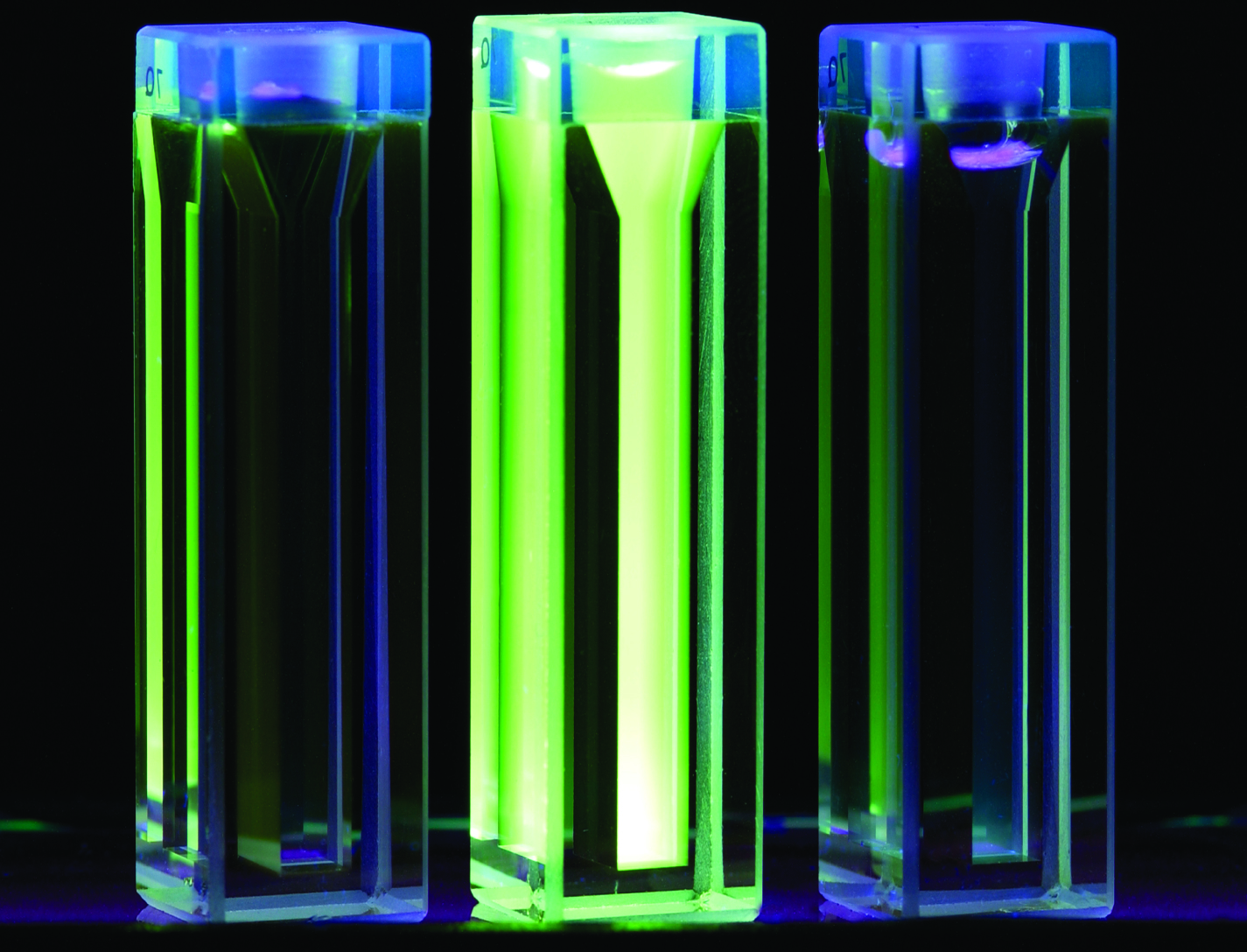
Gas Sensors Based on Coated and Doped Carbon Nanotubes
A typical sensor device includes a set of interdigitated microelectrodes fabricated by photolithography on silicon wafer or an electrically insulating substrate. In preparation for fabricating the SWCNT portion of such a sensor, a batch of treated (coated or doped) SWCNTs is dispersed in a solvent. The resulting suspension of SWCNTs is drop-deposited or injected onto the area containing the interdigitated electrodes. As the solvent evaporates, the SWCNTs form a mesh that connects the electrodes. The density of the SWCNTs in the mesh can be changed by varying the concentration of SWCNTs in the suspension and/or the amount of suspension dropped on the electrode area. To enable acquisition of measurements for comparison and to gain orthogonality in the sensor array, undoped SWCNTs can be similarly formed on another, identical set of interdigitated electrodes. Coating materials tested so far include chlorosulfonated polyethylene. Dopants that have been tested include Pd, Pt, Au, Cu and Rh nanoparticle clusters. To date, the sensor has been tested for NO2, NH3, CH4, Cl2, HCl, toluene, benzene, acetone, formaldehyde and nitrotoulene.
electrical and electronics
Robust High Temperature SiC Op Amps Practical Fabrication
The technology is part of a new generation of NASA Glenn SiC integrated circuits with unprecedented durability in the field of high-temperature electronics. For robust operational amplifiers based on SiC Junction Field Effect Transistors (JFETs), this novel compensation method mitigates issues with threshold voltage variations that are an effect of die location on the wafer. Modern high-temperature op amps on the market fall short due to temperature limits (only 225C for silicon-based devices). Previously, researchers noted that multiple op amps on a single SiC wafer had different amplification properties due to different threshold voltages that varied spatially as much as 18% depending on the circuit's distance from the SiC wafer center. While 18% is okay for some applications, other important system applications demand better precision. By applying this technology to the amplifier circuit design process, the op amp will provide the same signal gain no matter its position on the wafer. The compensation approach enables practical signal conditioning that works from 25C up to 500C.
sensors

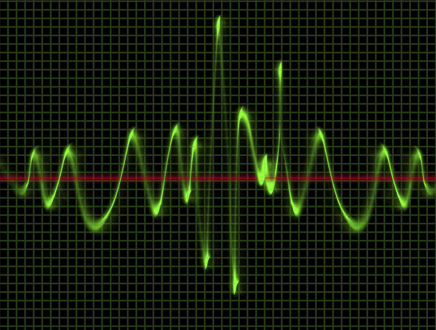
Method and Device for Biometric Verification and Identification
The advantage of using cardiac biometrics over existing methods is that heart signatures are more difficult to forge compared to other biometric devices. Iris scanners can be fooled by contact lenses and sunglasses, and a segment of the population does not have readable fingerprints due to age or working conditions. Previous electrocardiographic signals employed a single template and compared that template with new test templates by means of cross-correlation or linear-discriminant analysis.The benefit of this technology over competing cardiac biometric methods is that it is more reliable with a significant reduction in error rates. The benefit of this technology is that it creates a probabilistic model of the electrocardiographic features of a person instead of a single signal template of the average heartbeat. The probabilistic model described as Gaussian mixture model allows various modes of the feature distribution, in contrast to a template model that only characterizes a mean waveform. Another advantage is that the model uses both physiological and anatomical characterization of the heart, unlike other methods that mainly use only physiological characterization of the heart. By combining features from different leads, the heart of the person is better characterized in terms of anatomical orientation because each lead represents a different projection of the electrical vector of the heart. Thus, employing multiple electrocardiographic leads provides a better performance in subject verification or identification.
information technology and software

Otoacoustic Protection In Biologically-Inspired Systems
This innovation is an autonomic method capable of transmitting a neutralizing data signal to counteract a potentially harmful signal. This otoacoustic component of an autonomic unit can render a potentially harmful incoming signal inert. For selfmanaging systems, the technology can offer a selfdefense capability that brings new levels of automation and dependability to systems.
communications
Tunable Multi-Tone, Multi-Band, High-Frequency Synthesizer
Glenn's revolutionary new multi-tone, high-frequency synthesizer can enable a major upgrade in the design of high data rate, wide-band satellite communications links, in addition to the study of atmospheric effects. Conventional single-frequency beacon transmitters have a major limitation: they must assume that atmospheric attenuation and group delay effects are constant at all frequencies across the band of interest. Glenn's synthesizer overcomes this limitation by enabling measurements to be made at multiple frequencies across the entire multi-GHz wide frequency, providing much more accurate and actionable readings.
This novel synthesizer consists of a solid-state frequency comb or harmonic generator that uses step-recovery semiconductor diodes to generate a broad range of evenly spaced harmonic frequencies, which are coherent and tunable over a wide frequency range. These harmonics are then filtered by a tunable bandpass filter and amplified to the necessary power level by a tunable millimeter-wave power amplifier. Next, the amplified signals are transmitted as beacon signals from a satellite to a ground receiving station. By measuring the relative signal strength and phase at ground sites the atmospheric induced effects can be determined, enabling scientists to gather essential climate data on hurricanes and climate change. In addition, the synthesizer can serve as a wideband source in place of a satellite transponder, making it easier to downlink high volumes of collected data to the scientific community. Glenn's synthesizer enables a beacon transmitter that, from the economical CubeSat platform, offers simultaneous, fast, and more accurate wideband transmission from space through the Earth's atmosphere than has ever been possible before.
electrical and electronics
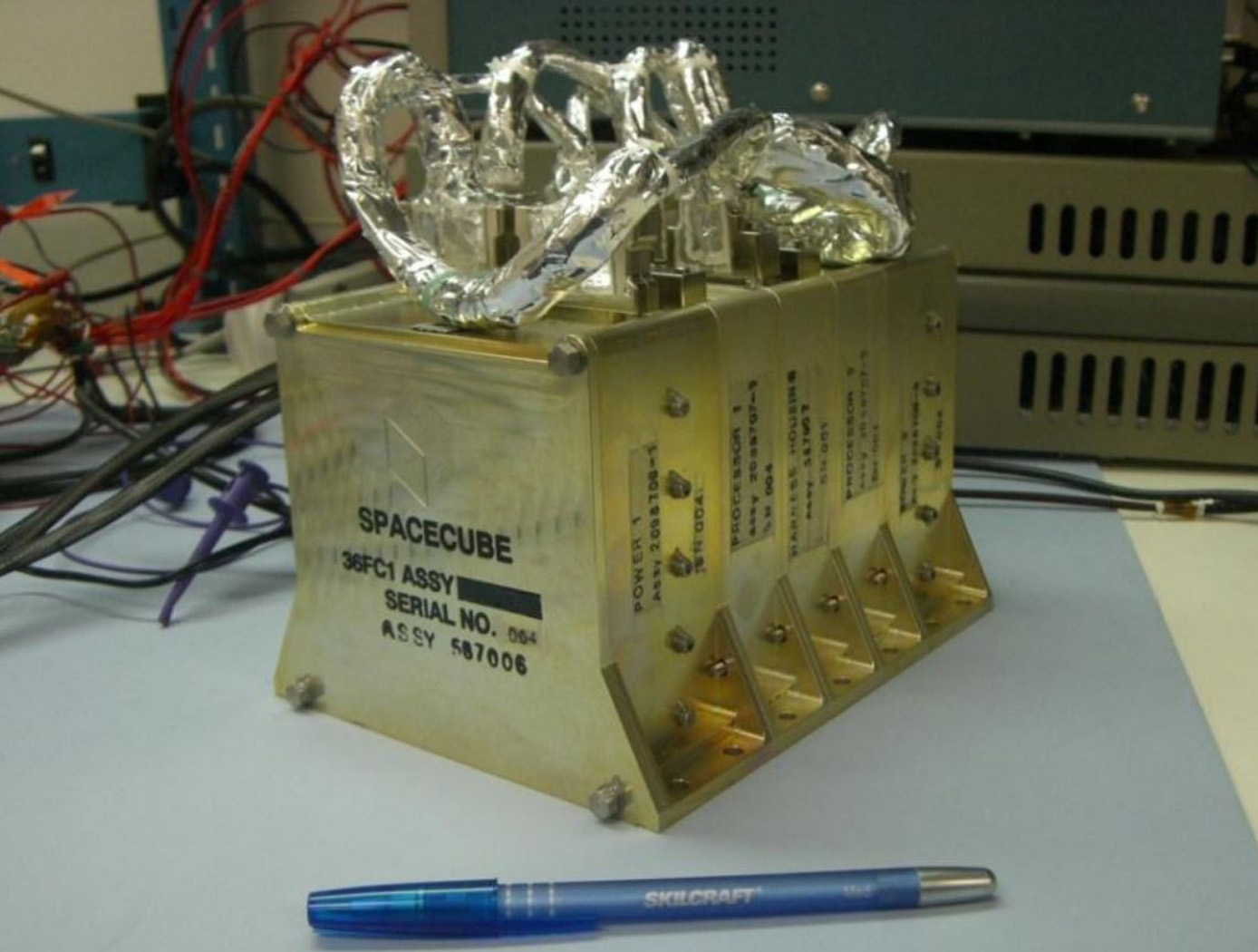
SpaceCube
Next generation instruments are capable of producing data at rates of 108 to 1011 bits per second, and both their instrument designs and mission operations concepts are severely constrained by data rate/volume. SpaceCube is an enabling technology for these next generation missions.
SpaceCube has demonstrated enabling capabilities in Earth Science, Planetary, Satellite Servicing, Astrophysics and Heliophysics prototype applications such as on-board product generation, intelligent data volume reduction, autonomous docking/landing, direct broadcast products, and data driven processing with the ability to autonomously detect and react to events. SpaceCube systems are currently being developed and proposed for platforms from small CubeSats to larger scale experiments on the ISS and standalone free-flyer missions, and are an ideal fit for cost constrained next generation applications due to the tremendous flexibility (both functional and interface compatibility) provided by the SpaceCube system.
Electrical and Electronics
Dynamic Range Enhancement of High-Speed Data Acquisition Systems
Electronic waveforms exist that exceed the capabilities of state-of-the-art data acquisition hardware that is commonly available. The electronic waveforms that need to be measured simultaneously contain wide bandwidth, high frequency content, a DC reference, high dynamic range, and a high crest factor. The NASA Glenn high-speed data acquisition system creates a voltage compression effect with a custom transfer function that is adapted to the voltage range, frequency bandwidth, and electrical impedance of both the test article and data acquisition device. The compression transfer function is later reversed (or decompressed) with a software algorithm to restore the original signal's voltage from the acquired data. The data is thus improved via better signal-to-noise ratio, better low-amplitude accuracy, better resolution, and preservation of high-frequency spectral content. The circuit can be realized with either passive components or both active and passive components. Either realization is specialized for the test article and data acquisition hardware.
This is an early-stage technology requiring additional development. Glenn welcomes co-development opportunities.

