Search
propulsion
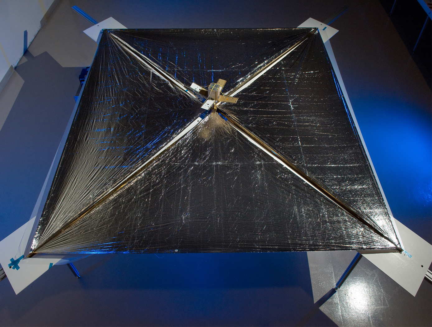
SMART Solar Sail
The SMART solar sail includes a reflective film stretched among nodes of a SMART space frame made partly of nanotubule struts. A microelectromechanical system (MEMS) at each vertex of the frame spools and unspools nanotubule struts between itself and neighboring nodes to vary the shape of the frame. The MEMSs is linked, either wirelessly or by thin wires within the struts, to an evolvable neural software system (ENSS) that controls the MEMSs to reconfigure the sail as needed. The solar sail is highly deformable from an initially highly compressed configuration, yet also capable of enabling very fine maneuvering of the spacecraft by means of small sail-surface deformations. The SMART Solar Sail is connected to the main body of the spacecraft by a SMART multi-tether structure, which includes MEMS actuators like those of the frame plus tethers in the form of longer versions of the struts in the frame.
Robotics Automation and Control

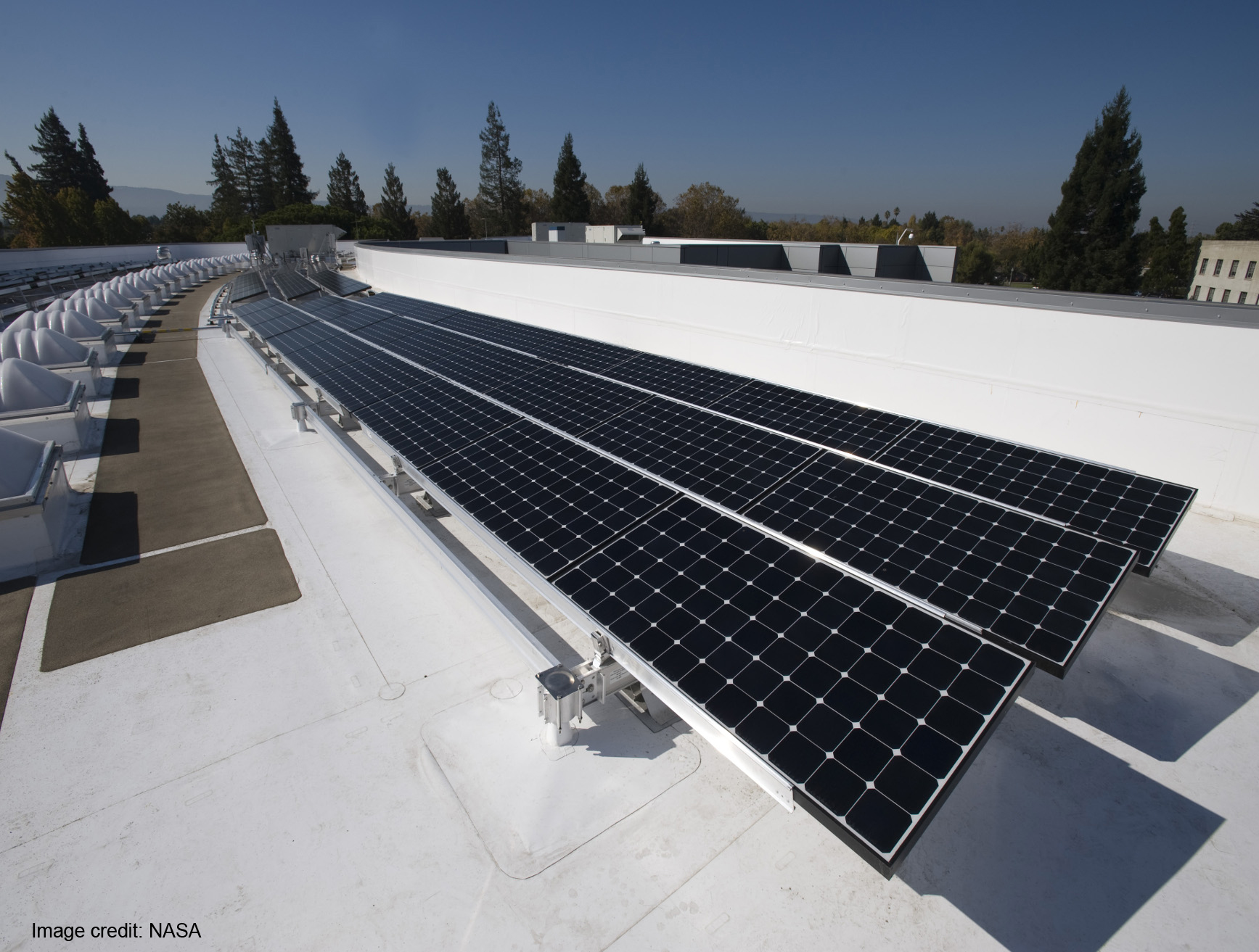
Robotic Assembly of Photovoltaic Arrays
NASA researchers have developed the PAPA technology to increase the efficiency of the thin-film solar array assembly process, significantly decreasing assembly time and labor costs associated with manufacturing large scale solar arrays. Traditional solar cell assembly is a labor intensive, multi-step, time-consuming process. This manual assembly will not be possible in a space environment. To enable solar array assembly in space, PAPA leverages robotic automation to distill the traditional assembly method into four fully automated steps: applying adhesive to block substrate, placing the solar cells using a vacuum tool attached to a universal robotic arm, printing the interconnects and buses to connect the cells, and applying a protective cover.
The PAPA technology is compatible with a variety of thin-film solar cells, including 3D printed cells (essential for future in-space manufacturing of arrays) and terrestrial manufacturing methods. As solar cell technologies mature, PAPA will be able to incorporate advancements into the paneling process. NASA researchers have begun to employ PAPA solar array fabrication and estimate savings of $300-$400/watt. For extraterrestrial assembly of solar panels the size of a football field or larger, PAPA could result in savings of approximately $500 million; a substantial cost savings driven by standardization and efficiency in the solar array assembly process. By demonstrating increases in assembly efficiency, time and cost savings, and passing multiple environmental exposure tests, the PAPA lab protype has completed the final phases of technology development and is ready for scale-up and commercialization.
electrical and electronics
High Mobility Transport Layer Structures for Rhombohedral Si/Ge/SiGe Devices
Performance of solar cells and other electronic devices such as transistors can be improved greatly if carrier mobility is increased. Si and Ge have Type-II bandgap alignment in cubically strained and relaxed layers. Quantum well and super lattice with Si, Ge, and SiGe have been good noble structures to build high electron mobility layer and high hole mobility layers. However, the atomic lattice constant of Ge is bigger than that of Si and direct epitaxial growth generates large density of misfit dislocations which decrease carrier mobility and shorten device life time. So it required special buffer layers such as super lattice or gradient indexed layers to grow Ge on Si wafers or Si on Ge wafers. The growth of these buffer layers takes extra effort and time such as post-annealing process to remove dislocations by dislocation gliding inside buffer layer.
This invention is a fabrication method for high mobility layer structures of rhombohedrally aligned SiGe on a trigonal substrate. The invention utilizes C-plane (0001) Sapphire which has a triangle plane, and a Si (Ge) (C) (111) crystal or an alloy of group TV semiconductor (111) crystal grown on the Sapphire.
power generation and storage

Solar Powered Carbon Dioxide (CO2) Conversion
This technology consists of a photoelectrochemical cell composed of thin metal oxide films. It uses sunlight (primarily the ultraviolet (UV), visible and Infrared (IR) portions)) and inexpensive titanium dioxide composites to perform the reaction. The device can be used to capture carbon dioxide produced in industrial processes before it is emitted to the atmosphere and convert it to a useful fuel such as methane. These devices can be deployed to the commercial market with low manufacturing and materials costs. They can be made extremely compact and efficient and used in sensor and detector applications.
Electrical and Electronics

Dynamic Range Enhancement of High-Speed Data Acquisition Systems
Electronic waveforms exist that exceed the capabilities of state-of-the-art data acquisition hardware that is commonly available. The electronic waveforms that need to be measured simultaneously contain wide bandwidth, high frequency content, a DC reference, high dynamic range, and a high crest factor. The NASA Glenn high-speed data acquisition system creates a voltage compression effect with a custom transfer function that is adapted to the voltage range, frequency bandwidth, and electrical impedance of both the test article and data acquisition device. The compression transfer function is later reversed (or decompressed) with a software algorithm to restore the original signal's voltage from the acquired data. The data is thus improved via better signal-to-noise ratio, better low-amplitude accuracy, better resolution, and preservation of high-frequency spectral content. The circuit can be realized with either passive components or both active and passive components. Either realization is specialized for the test article and data acquisition hardware.
This is an early-stage technology requiring additional development. Glenn welcomes co-development opportunities.
power generation and storage

Optimum Solar Conversion Cell Configurations
A solar cell manufactured from this new optical fiber has photovoltaic (PV) material integrated into the fiber to enable electricity generation from unused light, including non-visible portions of the spectrum and visible light not transmitted to a lighting application. These new solar cells are based around cylindrical optical fibers, providing two distinct advantages over the flat panels that lead to increased efficiency. The core fiber, used to transmit light, can be adjusted to increase or decrease the amount of available light that is transmitted to the lighting application at any point in real time. This invention can be applied wherever optical concentrators are used to collect and redirect incident light. Wavelengths as large as 780 nanometers (nm) can be used to drive the conversion process. This technology has very low operating costs and environmental impacts (in particular, no greenhouse gas emissions). The fiber uses low-cost polymer materials. It is lightweight and flexible, and can be manufactured using low-cost solution processing techniques. Such multifunctional materials have great potential for the future of solar and photovoltaic devices. They will enable new devices that are small and lightweight that can be used without connection to existing electrical grids.
propulsion

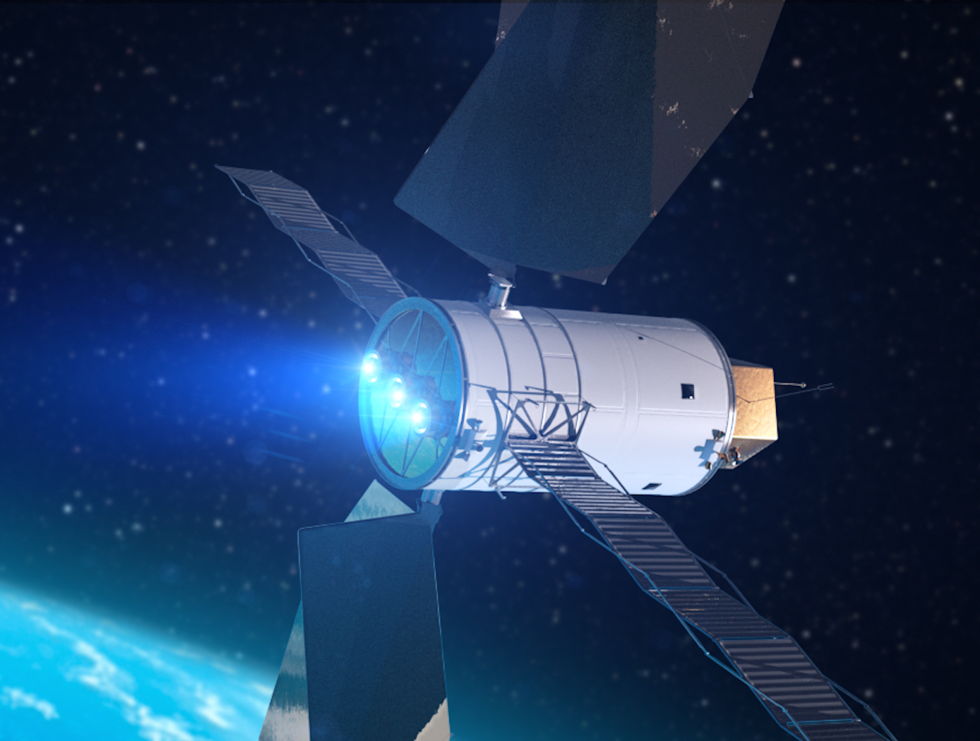
Power Processing Unit (PPU) for Small Spacecraft Electric Propulsion
Key subsystems of a scalable PPU for low-power Hall effect electric propulsion have been developed and demonstrated at NASA GRC. The PPU conditions and supplies power to the thruster and propellant flow control (PFC) components. It operates from an input voltage of 24 to 34 VDC to be compatible with typical small spacecraft with 28 V unregulated power systems. The PPU provides fault protection to protect the PPU, thruster, PFC components, and spacecraft. It is scalable to accommodate various power and operational requirements of low-power Hall effect thrusters. An important subsystem of a PPU is the discharge supply, which processes up to 95% of the power in the PPU and must process high voltage to accelerate thrust generating plasma. Each discharge power module in this PPU design is capable of processing up to 500 W of power and output up to 400 VDC. A full-bridge topology operating at switching frequency 50 kHz is used with a lightweight foil transformer. Two or more modules can operate in parallel to scale up the discharge power as required. Output voltage and current regulation controls allow for any of the common thruster start-up modes (hard, soft or glow).
<br><br><br>
Propulsion
Anode Manifold Plug for Hall Effect Thrusters
Flow-restricting features in a Hall thruster anode manifold assembly, typically precision manufactured orifices, can contribute to significant flow non-uniformity if tolerances on the features are not properly controlled. Non-uniformity in flow distribution negatively impacts thruster performance. The anode assembly is usually a complex and expensive assembly to manufacture. Removing the flow restricting elements from the anode manifold structure in favor of modular insertable subcomponents (i.e., plugs) enables the use of more reliable and repeatable precision manufacturing techniques. The resulting components can be tested, characterized, and sorted for acceptance before being installed into the larger anode assembly (i.e., quality control can be performed at the subcomponent level). This may lead to increased performance and yield rate of the final assembly.
The flow restrictor plugs can be made in many different ways. The most basic flow restrictor takes the form of a precision hole machined into a cylinder, where the cylinder is then press fit into a hole drilled into the anode base. Alternate embodiments of the flow restrictor include precision machined nozzles, laminar flow elements, or sintered porous metal elements. The flow restrictor can also be made from a different material than the anode base, such as a precision ruby orifice contained in a metal carrier which is installed in a metal anode base. The plugs can be installed in a variety of ways, all of which create hermetic seals. Installation can include a press fit relying on plastic deformation or threading the plug component into the anode base. Welding on the top surface of the anode base can also be done to provide a robust hermetic seal.
propulsion

High Propellant Throughput Small Spacecraft Electric Propulsion Thruster
NASAs High Propellant Throughput Small Spacecraft Electric Propulsion thruster offers a propellant throughput capability of greater than 120 kg with a nominal thruster efficiency greater than 50%. The new thruster design combines heritage Hall thruster component design approaches with recent NASA GRC advancements in the areas of advanced magnetic circuit design, robust propellant manifolds, and center mounted cathodes. Prototypes of the High Propellant Throughput Small Spacecraft Electric Propulsion thruster have been fabricated and proof-of-concept has been demonstrated.
A significant advancement in the High Propellant Throughput Small Spacecraft Electric Propulsion thruster is NASA's optimized magnetically shielded (OMS) field topology. The new OMS configuration reduces discharge channel erosion rates compared to conventional Hall thrusters, while reducing front pole cover erosion rates compared to traditional magnetically shielded Hall thrusters. This system also includes a largely unibody structure to reduce fabrication cost, increase strength, and optimize thermal management. A coupling plate between the high voltage discharge channel and low voltage thruster body allows more efficient thruster assembly and verification processes. Other design advancements further simplify assembly, improve robustness, and optimize performance.
power generation and storage

High-Efficiency Solar Cell
This NASA Glenn innovation is a novel multi-junction photovoltaic cell constructed using selenium as a bonding material sandwiched between a thin film multi-junction wafer and a silicon substrate wafer, enabling higher efficiencies. A multi-junction photovoltaic cell differs from a single junction cell in that it has multiple sub-cells (p-n junctions) and can convert more of the sun's energy into electricity as the light passes through each layer. To further improve the efficiencies, this cell has three junctions, where the top wafer is made from high solar energy absorbing materials that form a two-junction cell made from the III-V semiconductor family, and the bottom substrate remains as a simple silicon wafer. The selenium interlayer is applied between the top and bottom wafers, then pressure annealed at 221°C (the melting temperature of selenium), then cooled. The selenium interlayer acts as a connective layer between the top cell that absorbs the short-wavelength light and the bottom silicon-based cell that absorbs the longer wavelengths. The three-junction solar cell manufactured using selenium as the transparent interlayer has a higher efficiency, converting more than twice the energy into electricity than traditional cells. To obtain even higher efficiencies of over 40%, both the top and bottom layers can be multi-junction solar cells with the selenium layer sandwiched in between. The resultant high performance multi-junction photovoltaic cell with the selenium interlayer provides more power per unit area while utilizing a low-cost silicon-based substrate. This unprecedented combination of increased efficiency and cost savings has considerable commercial potential.
This is an early-stage technology requiring additional development. Glenn welcomes co-development opportunities.

