Miniaturized High-Speed Modulated X-Ray Source (MXS)
optics
Miniaturized High-Speed Modulated X-Ray Source (MXS) (GSC-TOPS-51)
Small, Low-Cost Option for High-Speed Modulation of X-Ray Intensity
Overview
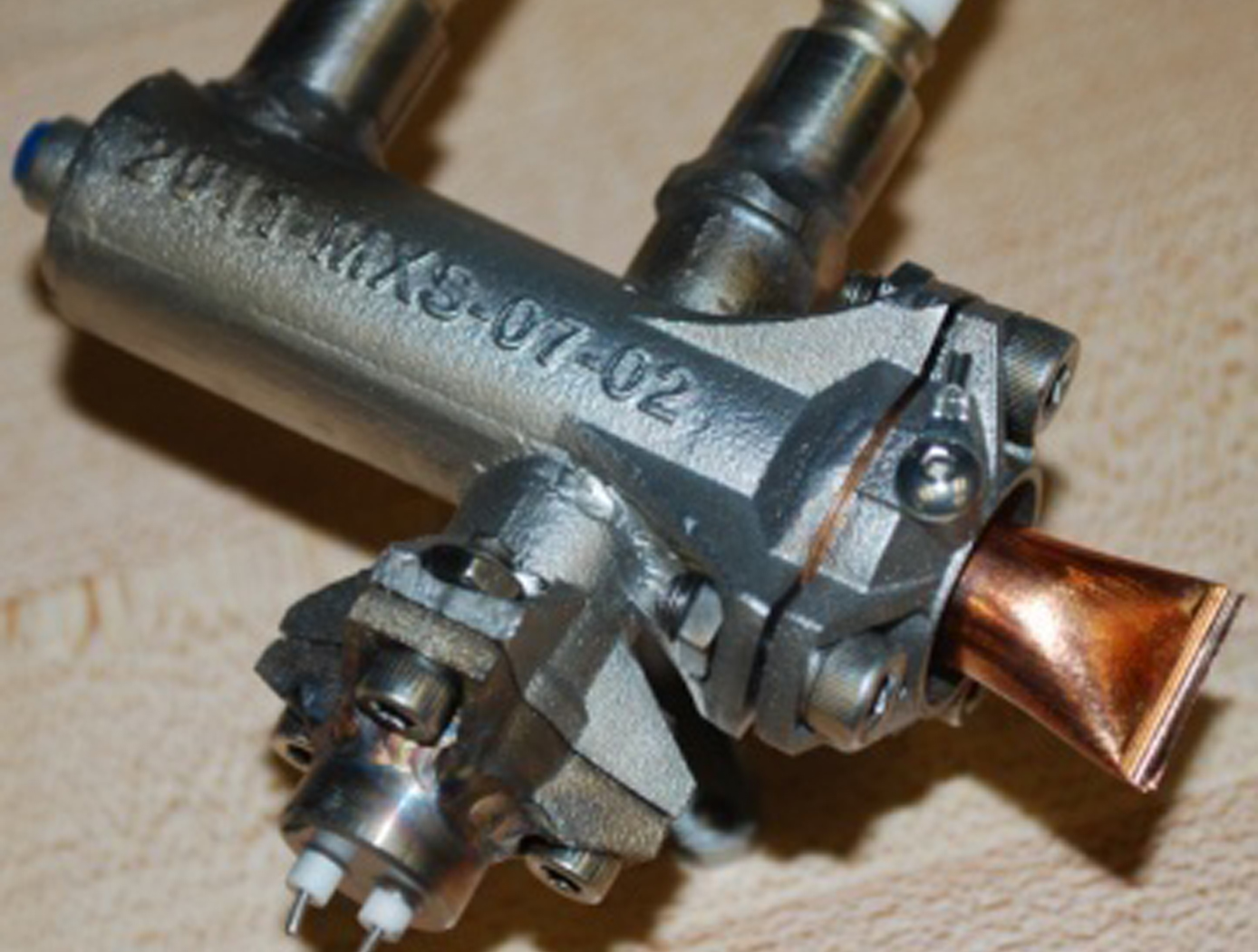
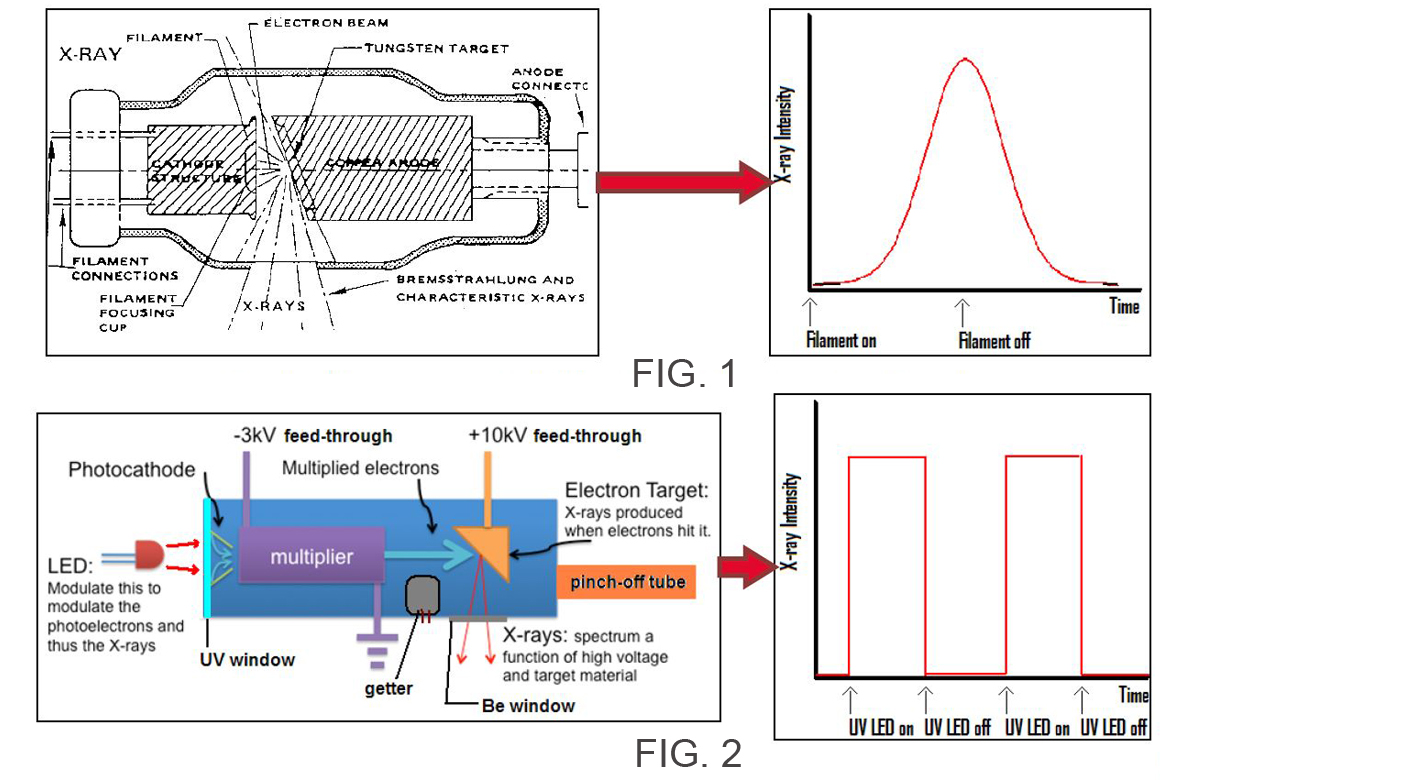
This miniaturized X-ray source can be modulated in intensity from completely off to full intensity, over 100 keV, in subnanosecond timescales. The high speed switching capability and miniature size make possible many new technologies including X-ray-based communication, compact time resolved X-ray diffraction, novel X-ray fluorescence instruments, low precise dose medical X-rays, and more.
The Technology
The MXS produces electrons by shining UV light from an LED onto a photocathode material such as magnesium. The electrons are then accelerated across several kV and into a chosen target material; deceleration produces X-rays characteristic of the target. The MXS uses an electron multiplier for high X-ray production efficiency.
The MXS is more compact, rugged, and power-efficient than standard X-ray sources. It can be manufactured using commercially available components and 3D printed housing, resulting in a low cost to manufacture. Unlike traditional X-ray sources, the MXS does not require a filament or vacuum and cooling systems. Most importantly, enabling rapid and arbitrary modulation allows using X-rays in the time domain, a new dimension to X-ray applications.


Benefits
- Arbitrary modulation from 0 to 100+ keV within a nanosecond
- Small size: Weighs around 160 g
- Low cost to produce
- Energy efficient
- Rugged: No filament burnout and no vacuum or cooling systems required
- Enables X-ray communication
- Secure, fast, and long-range
- More power efficient than current and next-gen laser-based space communication
- Works with hypersonic aircraft in atmosphere
Applications
- Secure, power-efficient X-ray-based communications
- In-flight calibration of X-ray detectors
- Compact, time-resolved X-ray diffraction and fluorescence
- Precise- and low-dose medical X-ray imaging
- Chemical/material analysis, resource identification (e.g., mining), and nondestructive testing (e.g., metal fatigue)
Similar Results

Low-Power Charged Particle Detector
Conventional scintillation radiation detectors make use of materials that emit light when hit by ionizing radiation. These large, bulky scintillators range anywhere from 6 inches to 6 feet in size. They are attached to glass photomultiplier tubes (PMTs), which are fragile, require high voltages, and are extremely sensitive to temperature changes. Conventional detectors also include a wave shifter (a material with a dopant to re-emit the scintillator light to match the sensitivity of the PMT or photodiode) which reduces efficiency and introduces unwanted weight and bulk.
Glenn's particle counter overcomes these challenges. A prototype was constructed from off-the-shelf components, and features a small scintillator (less than six inches long) and a low-voltage, UV-sensitive, wide-bandgap photodiode as the detector. Careful matching of the properties of the light emitted from the scintillator, and tailoring the sensitivity of the photodiode eliminates the need for a PMT and a wave shifter, not only saving space, weight, and power but also eliminating potential failure modes. By using wide-bandgap detectors, it can operate in changing temperature, vibration, pressure, and gravity conditions without need for a temperature compensation system. Built from solid-state components, Glenn's device is compact and robust.

X-Ray Diffraction Method to Detect Defects in Cubic Semiconductor (100) Wafers
This technology is a method of using x-ray diffraction (XRD) to evaluate the concentration of crystal structure defects, and thus the quality, of cubic (100)-oriented semiconductor wafers. Developed to enhance NASA's capabilities in fabricating chips for aeronautics applications, the method supplants existing methods that not only destroy the wafer in question, but can take as long as a day to determine the quality of a single wafer. The approach can be used with any commonly used semiconductor, including silicon, SiGe, GaAs and others, in a cubic (100) orientation, which covers at least 90% of commercial wafers. It can also be used to evaluate the quality of epi layers deposited on wafer substrates, and of ingots before they are sliced into wafers.

Sublimable Propellant Source for Iodine-fed Ion Propulsion System
NASAs iodine vapor feed system is based on a mechanism that holds and maintains the solid iodine is contact with a heated surface, in this case the walls of the propellant tank. The mechanism provides a robust and reliable steady-state delivery of sublimated iodine vapor to the ion propulsion system by ensuring good thermal contact between the solid iodine and the tank walls.
To date, the technology development effort includes extensive thermal, mechanical and flow modelling together with testing of components and subsystems required to feed iodine propellant to a 200-W Hall thruster. The feed system has been designed to use materials that are resistant to the highly-reactive nature of iodine propellant. Dynamic modeling indicates that the feed system tubing can be built is such a way as to reduce vibrationally-induced stresses that occur during launch. Thermal modeling has been performed to demonstrate that the feed system heater power levels are sufficient to heat the tank and propellant lines to operating temperatures, and sublime the iodine in the storage tank to supply propellant for reliable and long-term operation.

Multi-Layer Nuclear Thermionic Avalanche Cell
The Multi-Layer NTAC is comprised of a gamma-ray source and various layers of emitters, collectors, and insulators. Ideal emitter materials include elements with high atomic numbers, while ideal collector and insulator materials include elements with low atomic numbers. A high-energy gamma-ray (tens of keV to MeV) is used to liberate a large number of intra-band, inner-shell electrons from atoms within the emitter material for power generation through the primary interactions of photoelectric, Compton scattering, photonuclear, and electron/positron pair production processes. Secondary and tertiary electrons are liberated in the avalanche process as well. If a power conversion process effectively utilizes all liberated electrons in an avalanche mode through a power conversion circuit, the power output is drastically increased. Because power conversion is determined by the absorption rate of high energy photons, increasing power output requires either thicker collector material or a sufficient number of layer structures to capture the high energy photons, leaving no liberated electrons escaping (i.e., minimizing the leak of radioactive rays). The selection of materials, the thicknesses of the emitter, collector, and insulator, as well as the number of NTAC layers required are all determined by the energy of photon source. The thermal energy from radioactive decay can also be converted to electricity using a thermoelectric device to further increase power output. The Multi-Layer NTAC technology can be manufactured using existing semiconductor fabrication technology and can be tailored for small-to-large scale power needs, including kilowatt and megawatt applications.

X-Ray Crack Detectability
NASAs software technology uses an Image Quality Indicator (IQI)-based model that can predict whether cracks of a certain size can be detected, as well as a model that can provide appropriate conditions to optimize x-ray crack detection setup. Because this modeling software can predict minimum crack sizes that can be detected by a particular X-ray radiography testing setup, users can test various setups until the desired crack detection capabilities are achieved (predicted) by the modeling system.
These flaw size parameter models use a set of measured inputs, including thickness sensitivity, detector modulation transfer function, detector signal response function, and other setup geometry parameters, to predict the minimum crack sizes detectable by the testing setup and X-ray angle limits for detecting such flaws.
Current X-ray methods provide adequate control for detection of volumetric flaws but do not provide a high probability of detection (POD), and crack detection sensitivity cannot be verified for reliable detection. This results in reduced confidence in terms of crack detection. Given that these cracks, if undetected, can cause catastrophic failure in various systems (e.g., pressure vessels, etc.), verifying that X-ray radiography systems used for NDE can detect such cracks is of the utmost importance in many applications.


