Negative Dielectric Constant Material
materials and coatings
Negative Dielectric Constant Material (LAR-TOPS-177)
Method for a negative dielectric constant material based on ion conducting materials
Overview
NASA Langley Research Center has developed a novel negative dielectric constant material based on ion conducting materials. A negative dielectric constant material is an essential key for creating metamaterials, or artificial negative index materials (NIMs). NIMs have generated great attention due to their unique and exotic electromagnetic properties, and could be used for unique optical and microwave applications, including new methods of electromagnetic cloaking and extremely low loss communications.
The Technology
Metamaterials or artificial Negative Index Materials (NIM) are specially designed to exhibit a negative index of refraction, which is a property not found in any known naturally occurring material. These artificially configured composites have a potential to fill voids in the electromagnetic spectrum where conventional material cannot access a response, and enable the construction of novel devices such as microwave circuits and antenna components. The negative effective dielectric constant is a very important key for creating materials with a negative refractive index. However, current methods to achieve a negative effective dielectric constant are difficult to produce, not readily applicable to producing commercial metamaterials, and can have limited tunabilty.
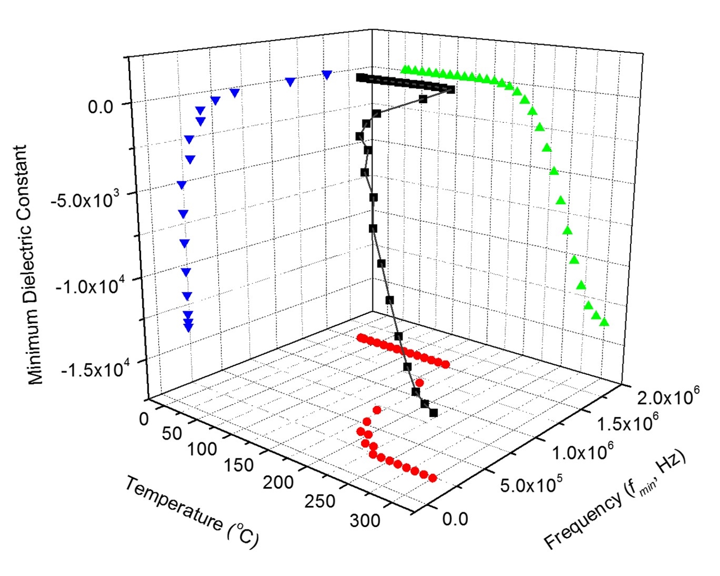
This invention is for a novel method to produce a material with a negative dielectric constant by doping ions into polymers, such as with a protonated poly(benzimidazole) (PBI), without complex geometric structures. The doped PBI shows a negative dielectric constant at megahertz (MHz) frequencies due to its reduced plasma frequency and an induction effect. The magnitude of the negative dielectric constant and the resonance frequency are tunable by dopant type and doping concentration.


Benefits
- Controllable resonance frequencies from radio to optical frequency
- Effective negative dielectric constant and resonance frequency can be controlled by dopant type, temperature, concentration and effective mass of dopant
- Can be used to create novel negative dielectric constant materials and negative index materials
- Molecular level homogenous metamaterials
Applications
- Super lenses (perfect lenses)
- Optical power limiting (eye protection from lasers)
- Optical switches and modulators
- Microwave waveguides and antennas, filters, and electromagnetic cloaking devices
- Perfect absorbers
- Nondestructive evaluation sensors (by enhancing sensitivity of the microwave nondestructive evaluation method)
Similar Results

Computer-implemented energy depletion radiation shielding
The difference between Layered Energy Depletion Radiation Shielding (LEDRS) and Stacked Energy Depletion Radiation Shielding (SEDRS) is how the piece of matter, or shield, is analyzed as radiation passes through the matter.
SEDRS involves using a defined and ordered stack of layers of shielding with different material properties such that the thickness and chemical properties of each material maximizes the absorption of energy from the radiation particles that are most damaging to the target. The SEDRS shielding method aims to provide the maximum level of energy absorption while still keeping shielding mass and volume low.
The process of LEDRS involves using layers of shielding material such that the thickness of each material is designed to absorb the maximum amount of energy from the radiation particles that are most damaging to the target after subsequent layers of shielding. The more energy is absorbed by the shielding material, the less energy will be deposited in the target minimizing the required mass to achieve a resulting lower dose for a given geometrical feature. The LEDRS shielding method aims to provide the maximum level of energy absorption. The process for designing LEDRS views potential radiation shields as a cascade of effects from each shielding layer to the next and is helpful for investigating the particular effects of each layer.
SEDRS and LEDRS can improve any technology that relies on the controlled manipulation of a radiation field by interaction with a material element.

Novel Radiation Shielding Material for Dramatically Extending the Orbit Life of Cubesats
A high density metal, such as tantalum or tungsten is coated onto thin aluminum sheet in precise ratios and thicknesses. The combined sheet is then easily formed into standardized enclosures compatible with CubeSat design and performance specifications.

NanoWire Glass Switch for Radio Frequency
The nanoionic-based switches developed by NASA's Glenn Research Center exploit the properties of some amorphous materials that can incorporate relatively large amounts of metal and behave as solid electrolytes. As with liquid electrolytes found in lead-acid batteries, for example, solid electrolytes consist of mobile ions which undergo oxidation/reduction reactions at the anode and cathode of the system. The ionic conductivity of such a material can be of the same order of magnitude as the electronic conductivity of a semiconductor but without the drawbacks of an electromechanical device.
In the nanoionic switch, ions are formed at an anode and migrate into the solid electrolyte, while electrons are injected from a cathode, thereby causing the growth of metal nanowires through the electrolyte from the cathode to the corresponding anode when a positive DC bias is applied. Once a nanowire has grown sufficiently to form an electrically conductive path between the electrodes, the switch is closed and no electric power is needed to maintain the connection, unlike in a MEMS or semiconductor-based switch. Moreover, the process of making the connection can easily be reversed by applying a negative bias, causing the wires to ungrow and the switch to open. Thus, NASA's state-of-the-art device is a reversible electrochemical switch that can have geometric features as small as nanometers. The process time for making or breaking the connection is very brief -- about a nanosecond. In addition, this nanoionic material can be deposited in such a way to form multilayer control circuits, which has the potential to minimize circuit footprints, reduce overall circuit losses, and provide unprecedented ease of integration.

Atomic Number (Z)-Grade Radiation Shields from Fiber Metal Laminates
This technology is a flexible, lighter weight radiation shield made from hybrid carbon/metal fabric and based on the Z-grading method of layering metal materials of differing atomic numbers to provide radiation protection for protons, electrons, and x-rays. To create this material, a high density metal is plasma spray-coated to carbon fiber. Another metal with less density is then plasma spray-coated, followed by another, and so on, until the material with the appropriate shielding properties is formed. Resins can be added to the material to provide structural adhesion, reducing the need for mechanical bonding. This material is amenable to molding and could be used to build custom radiation shielding to protect cabling and electronics in situations where traditional metal shielding is difficult to place.

Flexible Lightweight Radiation Shielding
The thin, lightweight radiation shielding is comprised of a low Z/high Z/low Z layered structure wherein the low Z layer is composed of titanium and the high Z layer is composed of either tantalum or antimony. Modelling of radiation shielding performance from a Cobalt 57 source shows a 10 times reduction in gamma radiation when using tantalum and a 25 times reduction when using antimony as compared with a single layer of lead. In addition, the Z-shielding is 25% lighter than a single lead layer with the same thickness (0.35-0.36 mm). The direct textile spraying innovation outlined by this invention enables the ability to shape this shielding into garments via the sewing of metal coated fibers. The refractory metal shielding can be added onto a variety of commodity-based fabrics including glass fabrics.


