Search
PATENT PORTFOLIO
Manufacturing
NASA's portfolio of manufacturing technology is a valuable resource for companies looking to improve their capabilities and bring innovative products to market. From aerospace and defense to healthcare and beyond, NASA's manufacturing technology can help you produce high-quality products that meet the most demanding requirements. So, if you're looking to take your manufacturing to new heights, NASA's portfolio of manufacturing technology might contain your solution.
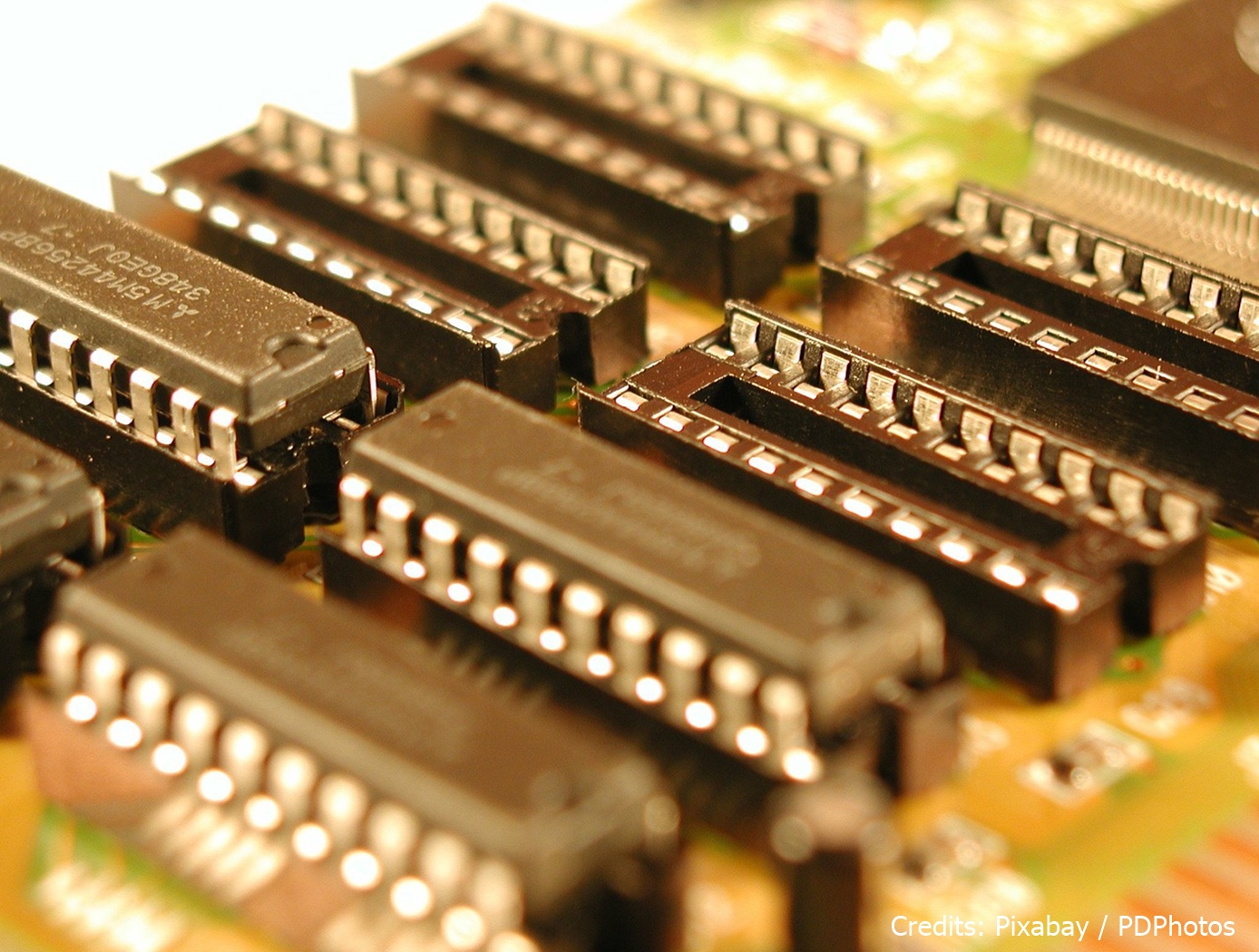
System for In-situ Defect Detection in Composites During Cure
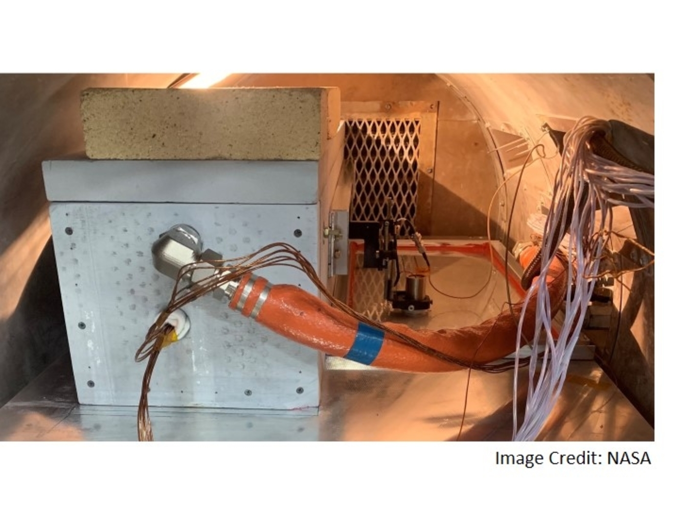
NASA's System for In-situ Defect (e.g., porosity, fiber waviness) Detection in Composites During Cure consists of an ultrasonic portable automated C-Scan system with an attached ultrasonic contact probe. This scanner is placed inside of an insulated vessel that protects the temperature-sensitive components of the scanner. A liquid nitrogen cooling systems keeps the interior of the vessel below 38°C. A motorized X-Y raster scanner is mounted inside an unsealed cooling container made of porous insulation boards with a cantilever scanning arm protruding out of the cooling container through a slot. The cooling container that houses the X-Y raster scanner is periodically cooled using a liquid nitrogen (LN2) delivery system. Flexible bellows in the slot opening of the box minimize heat transfer between the box and the external autoclave environment. The box and scanning arm are located on a precision cast tool plate. A thin layer of ultrasonic couplant is placed between the transducer and the tool plate. The composite parts are vacuum bagged on the other side of the tool plate and inspected. The scanning system inside of the vessel is connected to the controller outside of the autoclave. The system can provide A-scan, B-scan, and C-scan images of the composite panel at multiple times during the cure process.
The in-situ system provides higher resolution data to find, characterize, and track defects during cure better than other cure monitoring techniques. In addition, this system also shows the through-thickness location of any composite manufacturing defects during cure with real-time localization and tracking. This has been demonstrated for both intentionally introduced porosity (i.e., trapped during layup) as well processing induced porosity (e.g., resulting from uneven pressure distribution on a part). The technology can be used as a non-destructive evaluation system when making composite parts in in an oven or an autoclave, including thermosets, thermoplastics, composite laminates, high-temperature resins, and ceramics.
.jpg)
Interim, In Situ Additive Manufacturing Inspection
The in situ inspection technology for additive manufacturing combines different types of cameras strategically placed around the part to monitor its properties during construction. The IR cameras collect accurate temperature data to validate thermal math models, while the visual cameras obtain highly detailed data at the exact location of the laser to build accurate, as-built geometric models. Furthermore, certain adopted techniques (e.g., single to grouped pixels comparison to avoid bad/biased pixels) reduce false positive readings.
NASA has developed and tested prototypes in both laser-sintered plastic and metal processes. The technology detected errors due to stray powder sparking and material layer lifts. Furthermore, the technology has the potential to detect anomalies in the property profile that are caused by errors due to stress, power density issues, incomplete melting, voids, incomplete fill, and layer lift-up. Three-dimensional models of the printed parts were reconstructed using only the collected data, which demonstrates the success and potential of the technology to provide a deeper understanding of the laser-metal interactions. By monitoring the print, layer by layer, in real-time, users can pause the process and make corrections to the build as needed, reducing material, energy, and time wasted in nonconforming parts.

Ultrasonic Stir Welding
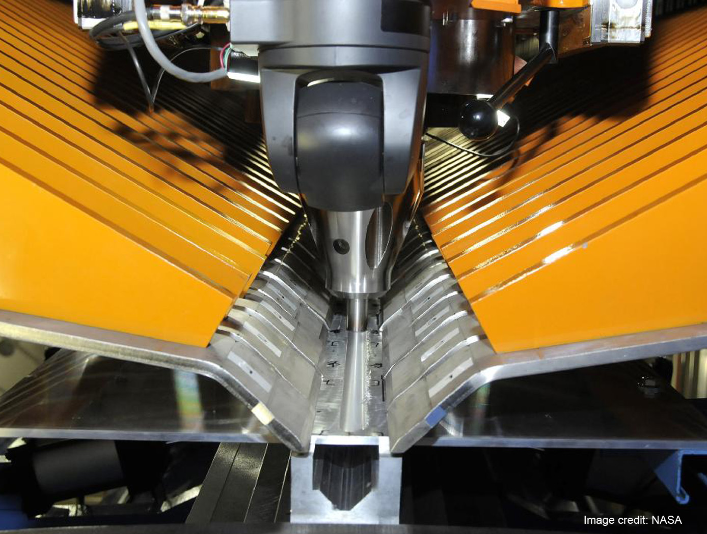
Ultrasonic Stir Welding is a solid state stir welding process, meaning that the weld work piece does not melt during the welding process. The process uses a stir rod to stir the plasticized abutting surfaces of two pieces of metallic alloy that forms the weld joint. Heating is done using a specially designed induction coil. The control system has the capability to pulse the high-power ultrasonic (HPU) energy of the stir rod on and off at different rates from 1-second pulses to 60-millisecond pulses. This pulsing capability allows the stir rod to act as a mechanical device (moving and stirring plasticized nugget material) when the HPU energy is off, and allowing the energized stir rod to transfer HPU energy into the weld nugget (to reduce forces, increase stir rod life, etc.) when the HPU energy is on. The process can be used to join high-melting-temperature alloys such as titanium, Inconel, and steel.

Fabrication of Fiber-Metal Laminates with Non-Autoclave Processes
The FMLs resulting from the NASA process have similar properties to traditionally produced metal/composite hybrid laminates including, as compared to either the composite or metal only structures, improved load carrying capability, lighter weight, improved stiffness, improved impact resistance and damage tolerance, and improved permeation resistance. The NASA process can be applied to various FML types, including GLARE (glass, aluminum, epoxy), and TIGR (titanium, graphite). Typical manufacturing processes are costly and complex shapes are hard to produce, whereby the NASA process enables use of these kinds of laminates without an autoclave or press, thus increasing the size that can be produced and decreasing the cost.
The resin pathways in the foils enable connection between the plies that can improve the interlaminar strength of the final part. Functionally the NASA process creates resin columns in the transverse direction of the plies. NASA is working to optimize the final properties by varying the size and distribution of the pathways.
Simplified Complimentary Metal-oxide-semiconductor Manufacturing Technique
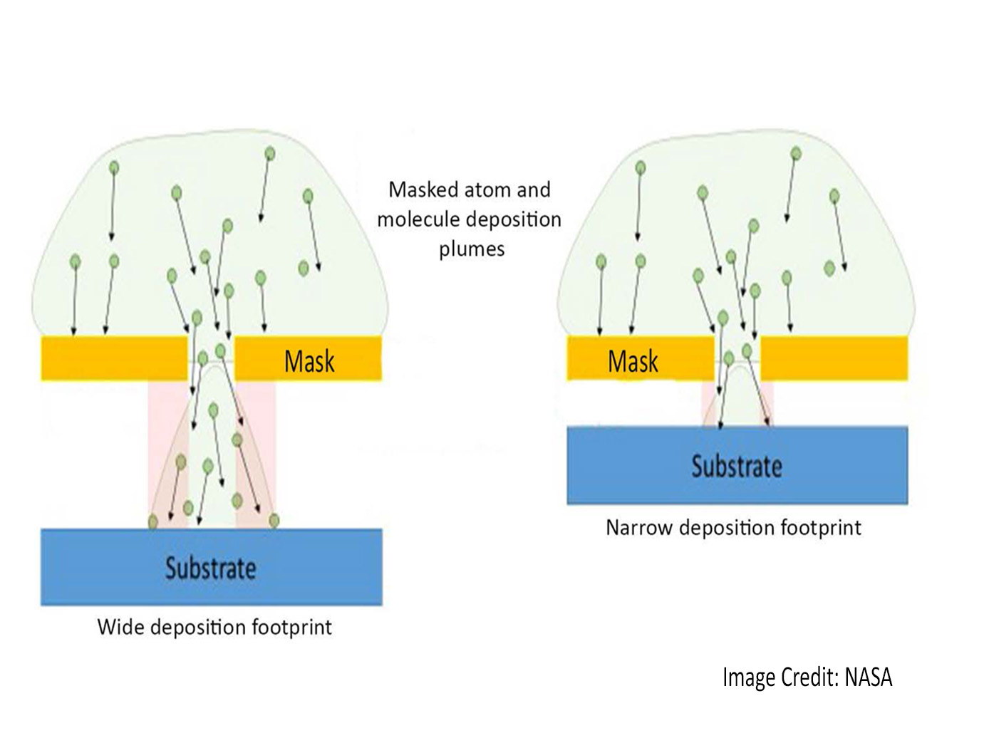
This innovation represents an alternative method to skip several of the conventional fabrication steps, using a mask designed to allow molecules in a sputtering plume to pass through openings engineered in the mask. This causes material to go where desired, without photoresist, and without selective etching, thus simplifying the process, reducing cost, chemical waste; and increasing throughput.
This method masks areas that do not need deposited material, causing local deposition instead. The shape and size are within tolerance. No etching steps, no photoresist patterning, and no metal removal is necessary. Other than planarization, selective deposition has replaced every step in the conventional process, accomplishing the same result in 8 steps instead of 19.
The technology can be easily used to fabricate custom chips and specialized sensors and devices that use the group III-V and II - VI semiconductor materials.
Abnormal Grain Growth Suppression in Aluminum Alloys
Heat treatment of the deformed welds is desirable in order to restore the properties of the alloy negatively affected in the weld region. In these alloys, abnormal grain growth frequently occurs in friction stir welds during solution heat treatment, and is known to degrade key materials properties, such as strength, ductility and toughness. The innovation of inserting an intermediate annealing step covered here reduces abnormal grain growth during post-welding heat treatment, thereby allowing optimum mechanical properties. This is important where Al-Li alloys (and other heat treatable alloys) are friction stir welded followed by deformation processing and high performance, high reliability structural components are required for aerospace vehicles.

Single Crystal SiGe/Sapphire Epitaxy
This innovation is based on a new fabrication method that alleviates the thermal loading requirement of the substrate, which previously required surface temperatures within the range of 850 to 900C. Our method employs a new thermal loading requirement of sapphire substrate for growing single crystal SiGe on sapphire substrate, in the range of 450 to 500C. SiGe/sapphire wafers produced via this process show a high reflectivity without the discoloration that appears in low quality films.
Improving Formability of Al-Li Alloys
Via this NASA innovation, a product is first heated to a temperature within the range of 204 to 343 degrees C for an extended soak of up to 16 hours. The product is then slowly heated to a second temperature within the range of 371 to 482 degrees C for a second soak of up to 12 hours. Finally, the product is slowly cooled to a final soak temperature of 204 to 343 degrees C before cooling to room temperature. The product so treated will exhibit greatly improved formability.
To date, the low formability issue has limited the use of lightweight Al-Li alloys for large rocket fuel tank dome applications. Manufacturing a dome by stretch forming typically requires multiple panels as well as multiple welding and inspection steps to assemble these panels into a full-scale fuel tank dome. Complex tensile and bending stresses induced during the stretch forming operations of Al-Li alloys have resulted in high rates of failure for this process. To spin form a large rocket dome, the spin blank must be prepared by joining smaller plates together using friction stir welding. However, friction stir welding produces a distinct metallurgical structure inside and around the friction stir weld that makes it very susceptible to cracking during spin forming.
X-Ray Diffraction Method to Detect Defects in Cubic Semiconductor (100) Wafers
This technology is a method of using x-ray diffraction (XRD) to evaluate the concentration of crystal structure defects, and thus the quality, of cubic (100)-oriented semiconductor wafers. Developed to enhance NASA's capabilities in fabricating chips for aeronautics applications, the method supplants existing methods that not only destroy the wafer in question, but can take as long as a day to determine the quality of a single wafer. The approach can be used with any commonly used semiconductor, including silicon, SiGe, GaAs and others, in a cubic (100) orientation, which covers at least 90% of commercial wafers. It can also be used to evaluate the quality of epi layers deposited on wafer substrates, and of ingots before they are sliced into wafers.
View more patents

